Organic light-emitting display device

A light-emitting display and organic technology, applied in the direction of electrical components, electrical solid devices, circuits, etc., can solve the problems of time-consuming, labor-intensive, complicated process, etc., and achieve the effects of simplifying the manufacturing process, improving the conductivity, and reducing the resistance

Inactive Publication Date: 2018-09-14
TCL CHINA STAR OPTOELECTRONICS TECH CO LTD
View PDF7 Cites 43 Cited by
  • Summary
  • Abstract
  • Description
  • Claims
  • Application Information

AI Technical Summary

Problems solved by technology

However, the inventors found that the pixel definition layer 2 of the organic light-emitting display device in the above method / and the inverted trapezoidal column foot a respectively need to be exposed and developed twice to form an upside-down trapezoidal structure, which is not only complicated in process, but also time-consuming and labor-intensive.

Method used


Image

  • Organic light-emitting display device
  • Organic light-emitting display device
  • Organic light-emitting display device

Examples


Embodiment Construction

[0060] In order to make the objectives, technical solutions and advantages of the present invention clearer, the present invention will be further described in detail below with reference to the accompanying drawings.

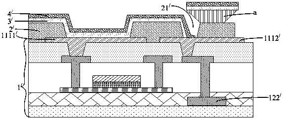
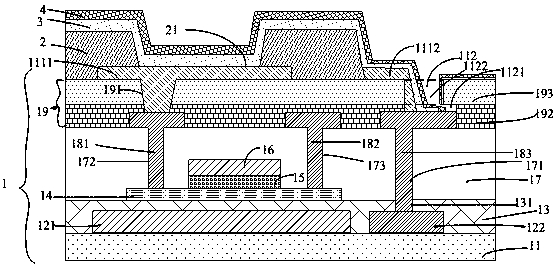
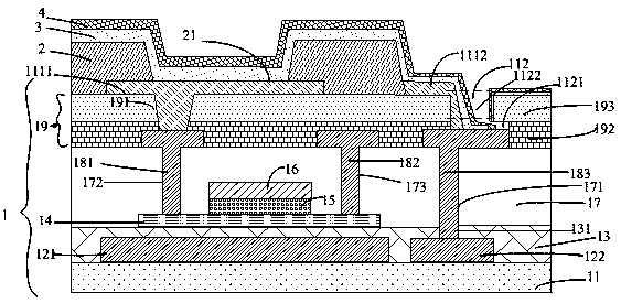
[0061] Such as figure 2 Shown here is an organic light-emitting display device provided in the first embodiment of the present invention, showing the structure when the array substrate in the organic light-emitting display device is a TFT array substrate with a double-gate structure, which specifically includes:

[0062] The array substrate 1 includes a pixel electrode 1111 and a metal connection electrode 1112 and an auxiliary electrode 122 located around the pixel electrode 1111; wherein the metal connection electrode 1112 is electrically connected through the recessed hole 112 and the auxiliary electrode 122 opened on the array substrate 1 Connection; the hole 112 is located above the auxiliary electrode 122, and is formed with a first cavity 1121 and a second ca...


PUM


Abstract

The invention provides an organic light-emitting display device which comprises an array substrate provided with a pixel electrode, a metal connection electrode and an auxiliary electrode; the metal connection electrode is connected with the auxiliary electrode through a concave hole positioned above the auxiliary electrode; the concave hole forms a first cavity and a second cavity which are interconnected, and the first cavity extends in the direction away from the pixel electrode from an edge line, away from one side of the pixel electrode, of the second cavity; a pixel definition layer is above the array substrate, and grooves corresponding to the concave hole and the pixel electrode are respectively reserved; an OLED semiconductor layer is above the pixel definition layer, covers the pixel electrode and the metal connection electrode and also extends into the first cavity to be connected with the auxiliary electrode; a cathode is above the OLED semiconductor layer, extends into thefirst cavity to be connected with the auxiliary electrode and is in a discontinuous connection state by taking the concave hole as a breaking point. Through the implementation of the organic light-emitting display device provided by the invention, the manufactory process can be simplified through omitting inverted trapezoidal column legs, the electrical conductivity of the cathode on the OLED semiconductor layer can be improved, and the purpose of reducing pressure drop is achieved.

Description

Technical field [0001] The present invention relates to the field of display technology, and in particular to an organic light emitting display device. Background technique [0002] Compared with the traditional LCD, the organic light-emitting display device is a self-luminous display device, because it does not require a backlight, it has the advantages of thinness, power saving, fast response, etc., and also has excellent viewing angle and contrast. Generally, an organic light emitting display device is composed of an array substrate and an OLED light emitting device disposed above the array substrate. The OLED light emitting device includes an anode, a hole injection layer, a hole transport layer, a light emitting layer, an electron transport layer, an electron injection layer, and a cathode; Among them, the anode, the hole injection layer, the hole transport layer, the light emitting layer, the electron transport layer, and the electron injection layer are formed as an OLED s...

Claims


Application Information

Patent Timeline
Patent Type & Authority Applications(China)
IPC IPC(8): H01L27/32H01L51/52
CPCH10K59/1315H10K50/824H01L29/78648H01L29/78633H10K59/124H10K59/1213H10K59/1201H01L27/1225H10K59/122H10K50/8445H10K59/131
Inventor 卢马才
Owner TCL CHINA STAR OPTOELECTRONICS TECH CO LTD
Why Eureka
Try Eureka