
OLED backboard and manufacturing method thereof

A manufacturing method and backplane technology, applied in the field of OLED backplane and OLED backplane production, can solve the problems of high production cost and restrictions on large-scale commercialization of OLED displays, and achieve low production cost, avoiding the influence of light, and simple structure Effect

Active Publication Date: 2018-09-14
TCL CHINA STAR OPTOELECTRONICS TECH CO LTD
View PDF3 Cites 5 Cited by
  • Summary
  • Abstract
  • Description
  • Claims
  • Application Information

AI Technical Summary

Problems solved by technology

However, due to the high cost of vacuum thermal evaporation preparation, the large-scale commercialization of OLED displays is limited.

Method used


Image

  • OLED backboard and manufacturing method thereof
  • OLED backboard and manufacturing method thereof
  • OLED backboard and manufacturing method thereof

Examples


Embodiment Construction

[0035] In order to further explain the technical means adopted by the present invention and its effects, the following describes in detail the preferred embodiments of the present invention and the accompanying drawings.

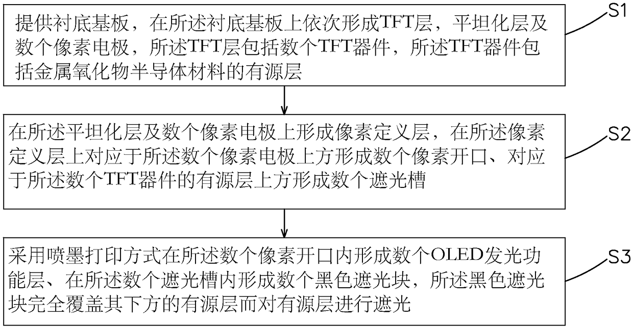
[0036] See figure 1 , The present invention first provides a method for manufacturing an OLED backplane, including the following steps:

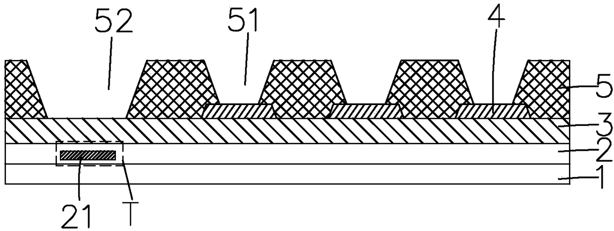
[0037] Step S1, such as figure 2 As shown, a base substrate 1 is provided, a TFT layer 2 is formed on the base substrate 1, a planarization layer 3 is formed on the TFT layer 2, and a number of pixel electrodes 4 are formed on the planarization layer 3; The TFT layer 2 includes several TFT devices T, and the TFT devices T include an active layer 21, and the material of the active layer 21 is a metal oxide semiconductor material.

[0038] Specifically, in the step S1, the material of the active layer 21 may be indium gallium zinc oxide (IGZO), indium zinc tin oxide (IZTO), indium gallium zinc tin oxide (IGZTO) and other metal oxi...


PUM


Abstract

The invention provides an OLED backboard and a manufacturing method thereof. According to the manufacturing method, pixel openings and shading grooves positioned over an active layer correspondingly are formed in a pixel definition layer, and OLED light emitting function layers are formed in the pixel openings respectively and black shading blocks covering the active layers completely are formed in the shading grooves respectively in an ink jetting manner. A TFT device is avoided from influence of illumination, characteristics of the TFT device are ensured, technology is simple and the production cost is low.

Description

Technical field [0001] The present invention relates to the field of display technology, in particular to a manufacturing method of an OLED backplane and an OLED backplane. Background technique [0002] Flat panel display devices have many advantages such as thin body, power saving, and no radiation, and have been widely used. The existing flat panel display devices mainly include liquid crystal display (Liquid Crystal Display, LCD) and organic light emission display (Organic Light Emitting Display, OLED). [0003] LCD display devices are widely used in various consumer electronics such as mobile phones, televisions, personal digital assistants, digital cameras, notebook computers, desktop computers, etc. due to their advantages of high image quality, power saving, thin body and wide application range. Products have become the mainstream in display devices. The OLED display device is an actively luminous display, which has the advantages of self-luminescence, high contrast, wide ...

Claims


Application Information

Patent Timeline
Patent Type & Authority Applications(China)
IPC IPC(8): H01L27/32
CPCH10K59/121H10K59/122H10K71/135H10K59/126H10K59/1201H10K71/00H10K2102/102H10K2102/103
Inventor 周星宇
Owner TCL CHINA STAR OPTOELECTRONICS TECH CO LTD
Learn More