Display panel and fabrication method thereof
A technology for a display panel and a manufacturing method, which is used in the manufacture of semiconductor/solid-state devices, organic semiconductor devices, electrical components, etc., can solve the problems of poor stress flexibility, complicated processes, and high price of photomasks, so as to reduce production costs and ensure Flexibility, the effect of simplifying the process
- Summary
- Abstract
- Description
- Claims
- Application Information
AI Technical Summary
Problems solved by technology
Method used
Image
Examples
Embodiment 1
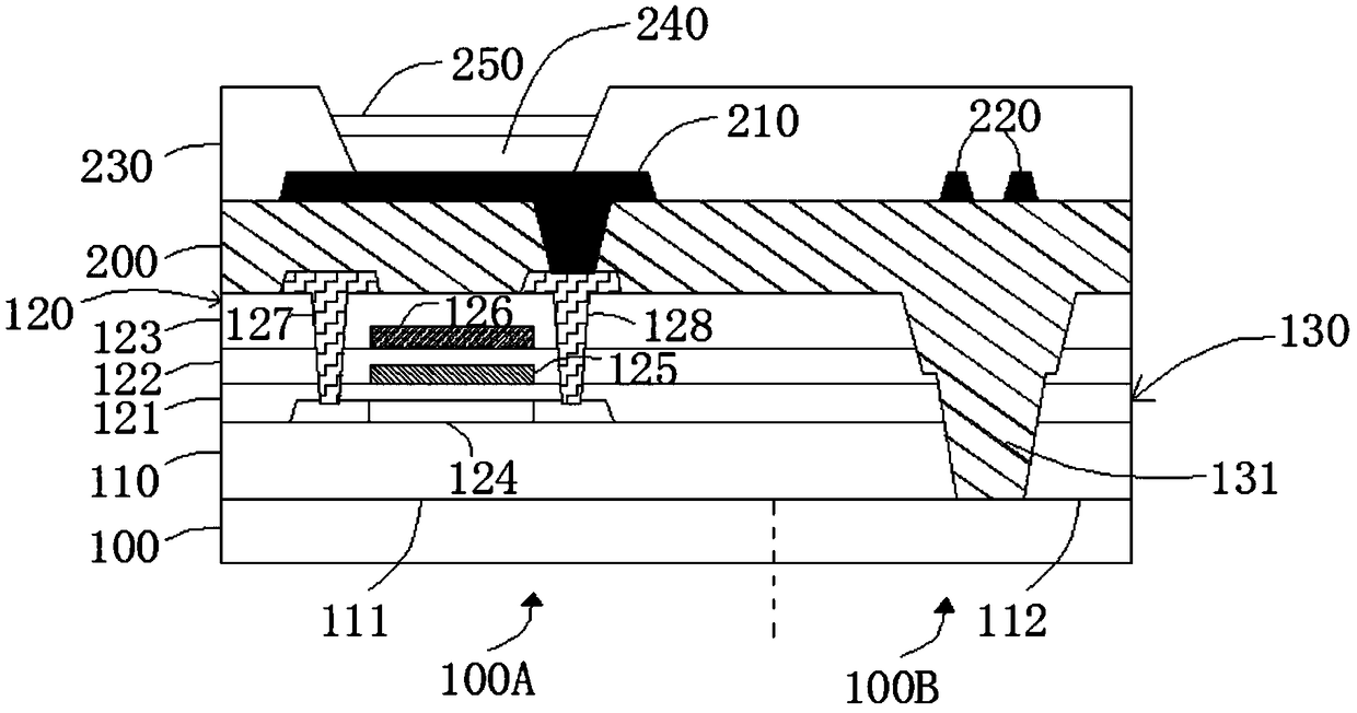
[0062] figure 1 is a schematic structural diagram of a display panel according to Embodiment 1 of the present invention.
[0063] refer to figure 1As shown, the first embodiment of the present invention provides a display panel. The display panel includes: a substrate 100 , a buffer layer 110 , a thin film transistor layer 120 , a composite insulating layer 130 and a flat layer 200 . However, it can be understood that the present invention is not limited thereto, and the display panel according to the embodiment of the present invention may also include other necessary components.
[0064] Specifically, the substrate 100 includes a display area 100A and a bending area 100B.
[0065] The buffer layer 110 is disposed on the substrate 100 . The buffer layer 110 includes a first buffer layer 111 located in the display area 100A and a second buffer layer 112 located in the bending area 100B.
Embodiment approach
[0066] The thin film transistor 120 is disposed on the first buffer layer 111 . As an embodiment of the present invention, the thin film transistor 120 includes: an active layer 124, a first insulating layer 121, a gate 125, a second insulating layer 122, a capacitor electrode 126, an interlayer insulating layer 123, a source 127 and a drain Pole 128.
[0067] Specifically, the active layer 124 is disposed on the first buffer layer 111 . The first insulating layer 121 is disposed on the active layer 124 and the first buffer layer 121 , and the first insulating layer 121 extends into the bending region 100B. The gate 125 is disposed on the first insulating layer 121 , and in this embodiment, the gate 125 can also serve as a second capacitor electrode to form a storage capacitor (not shown) with the first capacitor electrode 126 . The second insulating layer 122 is disposed on the gate 125 and the first insulating layer 121 , and the second insulating layer 122 extends into th...
Embodiment 2
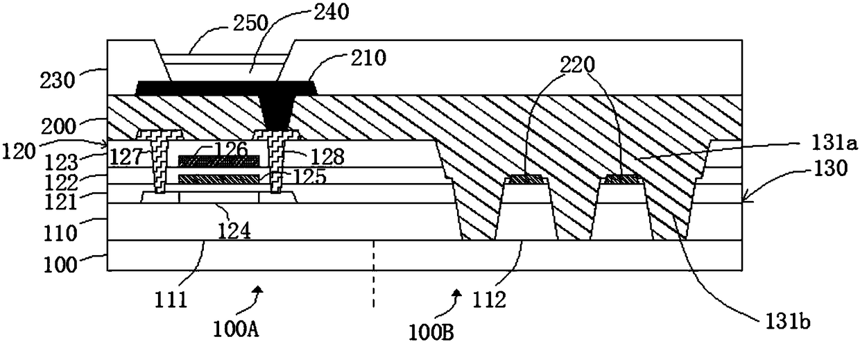
[0075] figure 2 is a schematic structural diagram of a display panel according to Embodiment 2 of the present invention.
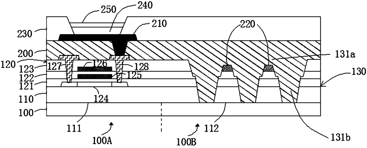
[0076] refer to figure 2 As shown, the difference between the display panel proposed by the second embodiment of the present invention and the first embodiment is that the via hole 131 in the second embodiment of the present invention includes: a hole that penetrates the interlayer insulating layer 123 and the second insulating layer 122 The first via hole 131 a, and a plurality of second via holes 131 b extending from the bottom of the first via hole 131 a through the first insulating layer 121 and the second buffer layer 112 . As an embodiment of the present invention, one first via hole 131 a and three second via holes 131 b extending from the bottom of the first via hole 131 a through the first insulating layer 121 and the second buffer layer 112 are provided.
[0077] In this embodiment, the wiring 220 is disposed on the first insulating layer 121...
PUM
 Abstract
Description
Claims
Application Information


