A buffer circuit for a low noise mems microphone
A microphone and buffer technology, applied in the electronic field, can solve the problems of high noise, large chip area occupied, large power consumption, etc., and achieve the effects of suppressing 1/f noise, reducing system imbalance, and reducing occupied area
- Summary
- Abstract
- Description
- Claims
- Application Information
AI Technical Summary
Problems solved by technology
Method used
Image
Examples
Embodiment Construction
[0014] The present invention will be further described below in conjunction with the accompanying drawings.
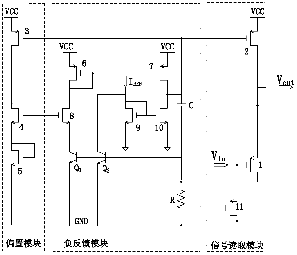
[0015] refer to figure 1 , to further describe the specific circuit of the present invention.
[0016] By the electrical schematic diagram of the present invention figure 1 The dotted line in the figure divides the electrical schematic diagram of the present invention into three parts: a bias module, a negative feedback module, and a signal reading module.
[0017] Electrical schematic diagram of the present invention figure 1 The bias module described by the dotted line in includes a PMOS transistor 3, two NMOS transistors 4 and 5, the output terminal of the bias module is connected to the input terminal of the negative feedback module, and the input terminal of the bias module is connected to the negative feedback module output connection.
[0018] The gate of the PMOS transistor 3 in the bias module is respectively connected to the drain of the second PMOS trans...
PUM
 Abstract
Description
Claims
Application Information


