Flash memory chip testing method and system

A technology of flash memory chips and testing methods, applied in static memory, instruments, etc., can solve problems such as reducing measurement accuracy

Active Publication Date: 2018-09-21
GIGADEVICE SEMICON (BEIJING) INC +1
View PDF4 Cites 5 Cited by
  • Summary
  • Abstract
  • Description
  • Claims
  • Application Information

AI Technical Summary

Problems solved by technology

[0007] The present invention provides a flash memory chip testing method and system to solve the problem of reducing

Method used


Image

  • Flash memory chip testing method and system
  • Flash memory chip testing method and system
  • Flash memory chip testing method and system

Examples


Embodiment 1

[0085] refer to Figure 4 , shows a flow chart of the flash memory chip testing method in Embodiment 1 of the present invention, which may specifically include the following steps:

[0086] Step 101, the PMU measurement unit receives a first output instruction sent by the PC; wherein, the first output instruction includes: a first output voltage instruction or a first output current instruction.

[0087] In the embodiment of the present invention, the PMU measurement unit is connected to a PC, and the PC is used to control the PMU measurement unit. The user may input the first output instruction according to a preset format on the PC, wherein the first output instruction may indicate the output voltage value or the output current value of the PMU measurement unit. At the same time, the output instruction may also include: the change speed of the output voltage value or current value, which is not limited in the present invention.

[0088] Step 102, the PMU measurement unit p...

Embodiment 2

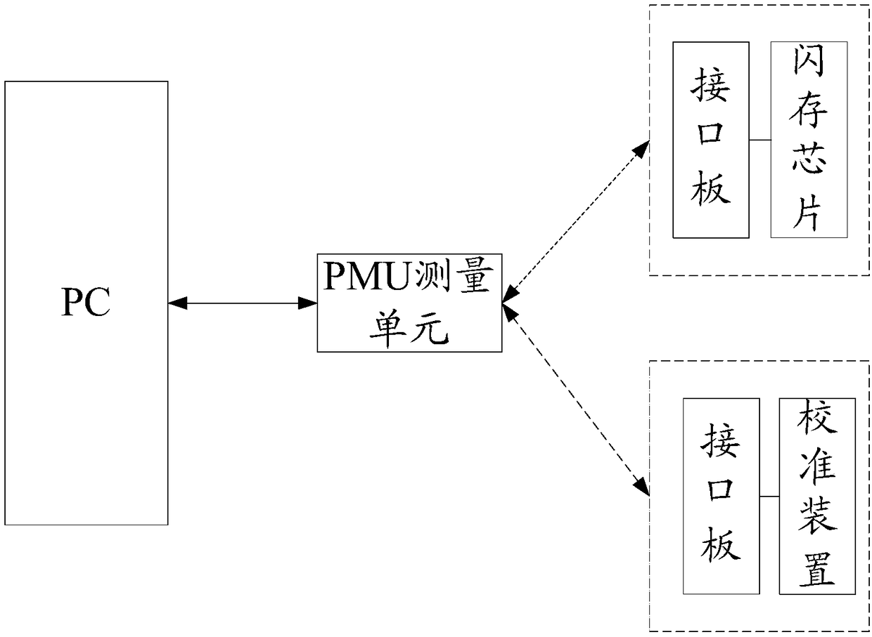
[0109] refer to Figure 5 , The system of the present invention further includes a high-precision measuring instrument; wherein, the high-precision measuring instrument is connected to the interface board of the calibration device, and the high-precision measuring instrument is connected to the PC.

[0110] refer to Figure 6 , which shows a flow chart of a method for calibrating a flash memory chip according to Embodiment 2 of the present invention, which may specifically include the following steps:

[0111] Step 201, the PMU measurement unit receives a second output command sent by the PC; wherein the second output command includes: a second output voltage command or a second output current command.

[0112] Refer to step 101, which will not be described in detail here.

[0113] Step 202, the PMU measurement unit provides a stable second initial power supply to the calibration device interface board according to the second output instruction; wherein, the second initial p...

Embodiment 3

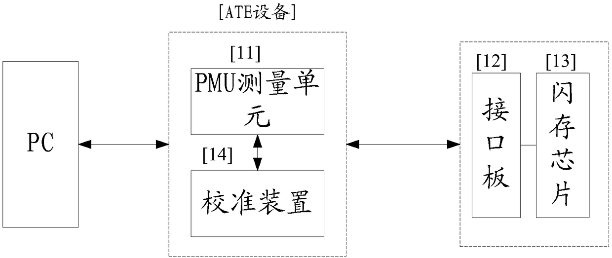
[0128] refer to Figure 7 , shows a structural block diagram of a flash memory chip testing system according to Embodiment 3 of the present invention, the system includes: PC310, PMU measurement unit 320, calibration device interface board 330, flash memory chip interface board 340; wherein, the calibration The device interface board 330 includes: a calibration device 331 and an interface board 332; the calibration device interface board 330 is connected to the PMU measurement unit 320; the PMU measurement unit 320 is connected to the PC310; the flash memory chip interface board 340 and the The interface board 330 of the calibration device is equivalently replaced;

[0129] Described flash memory chip testing system also comprises:

[0130] The first receiving module 321 is used for the PMU measurement unit to receive the first output instruction sent by the PC; wherein, the first output instruction includes: a first output voltage instruction or a first output current instru...


PUM


Abstract

The embodiment of the invention provides a flash memory chip testing method and system and relates to the field of chip testing technology. The method comprises the steps that a calibration device interface board is connected with a PMU (Parametric Measurement Unit); the PMU is connected with a PC; the calibration device interface board is replaced with a flash memory chip interface board at the same position; the PMU receives a first output instruction sent by the PC; the PMU supplies a stable first initial power source to the calibration device interface board; the PMU tests a first test voltage and a first test current corresponding to a calibration device at the same time; the PMU feeds the first test voltage and the first test current back to the PC; the PC configures a first calibration parameter; and then the PMU is calibrated. Since the calibration device interface board is replaced with the flash memory chip interface board at the same position for testing of a flash memory chip, automatic calibration can be realized, meanwhile, a calibration line is consistent with an actual test line, and the measurement precision of the flash memory chip is improved.

Description

technical field [0001] The invention relates to the technical field of chip testing, in particular to a flash memory chip testing method and system. Background technique [0002] In the chip debugging stage of flash memory, in the test of some internal threshold voltage and conduction current, the test accuracy needs to reach the precision scale of 1mv small voltage or 1uA small current, which requires relatively high accuracy of the test instrument. [0003] In the field of flash memory chip voltage and current measurement, generally use figure 1 The principle of parameter measurement, this structure is called Kelvin connection. From left to right is the power supply line, which is responsible for providing power to the back-end device under test. Below, from right to left, are the measurement channels, which are responsible for feeding back the implemented DC parameters to the control terminal. [0004] exist figure 1 In [05], the actual voltage value of the load termi...

Claims


Application Information

Patent Timeline
IPC IPC(8): G11C29/56
CPCG11C29/56
Inventor 蔡德智王永成韩飞
Owner GIGADEVICE SEMICON (BEIJING) INC
Why Eureka
Try Eureka