Inkjet printing OLED display panel and preparation method thereof

An inkjet printing and display panel technology, which is applied in semiconductor/solid-state device manufacturing, electrical components, electrical solid-state devices, etc., can solve problems such as the degradation of thin-film transistor devices, achieve the suppression of threshold voltage drift, save photomasks, and save preparation time and cost effects

Active Publication Date: 2018-09-21
SHENZHEN CHINA STAR OPTOELECTRONICS SEMICON DISPLAY TECH CO LTD
View PDF4 Cites 7 Cited by
  • Summary
  • Abstract
  • Description
  • Claims
  • Application Information

AI Technical Summary

Problems solved by technology

It has been verified that the SiO process will cause deterioration of thin film transistor devices

Method used


Image

  • Inkjet printing OLED display panel and preparation method thereof
  • Inkjet printing OLED display panel and preparation method thereof
  • Inkjet printing OLED display panel and preparation method thereof

Examples


Embodiment Construction

[0040] The present invention provides a kind of preparation method of the OLED display panel of inkjet printing, and this preparation method comprises the following steps:

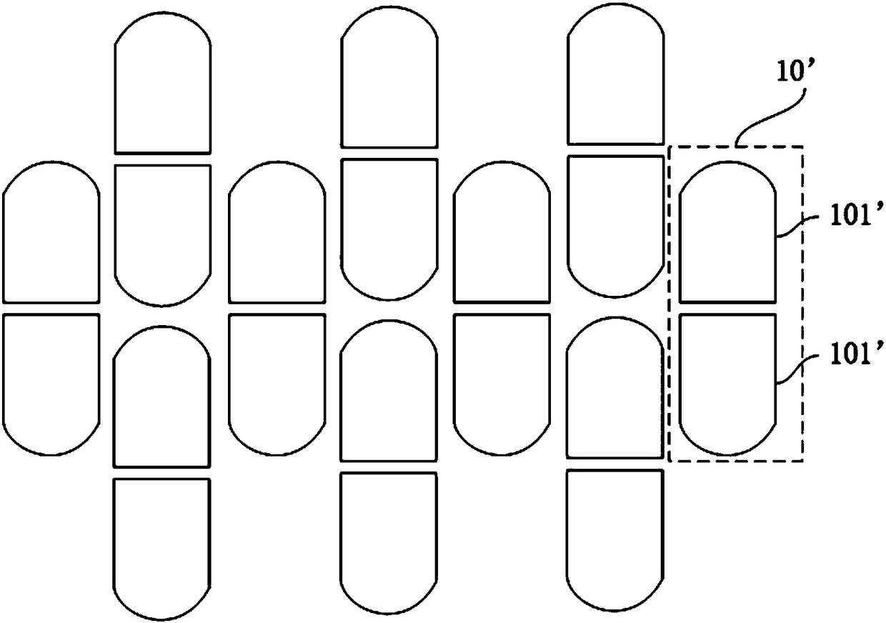
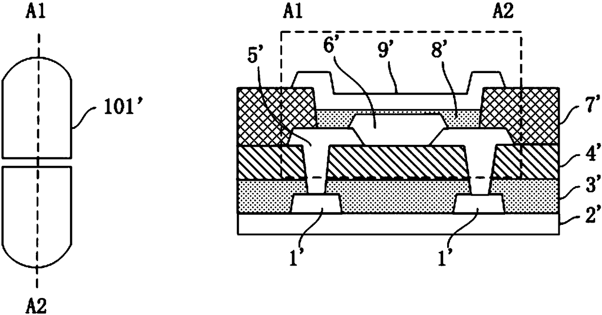
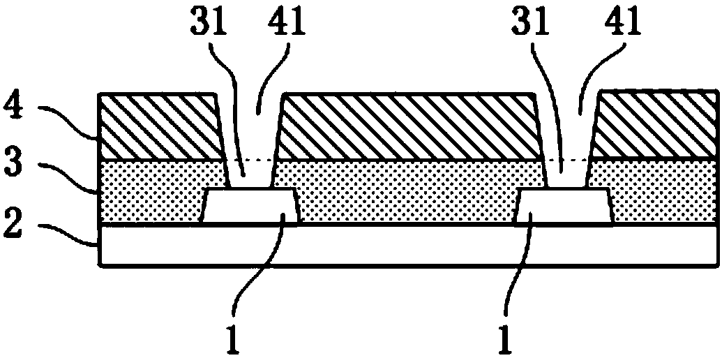
[0041] Such as image 3 As shown, at least one pair of thin film transistors 1 are prepared on a glass substrate 2;

[0042] Depositing a passivation layer 3 on the glass substrate 2, the passivation layer 3 covers at least one pair of thin film transistors 1;

[0043] depositing a planarization layer 4 on the passivation layer 3;

[0044] At least one pair of via holes are formed on the passivation layer 3 and the planar layer 4, and the via holes 31 on the passivation layer 3 are opposite to the via holes 41 on the planar layer 4 and the via holes 31 on the passivation layer 3 are opposite to the via holes 41 on the planar layer 4. The via holes 41 on the planar layer 4 are located above at least one pair of thin film transistors 1;

[0045] Such as Figure 4 As shown, at least one pair of anodes 5 a...


PUM


Abstract

The invention provides an inkjet printing OLED display panel and a preparation method thereof. The method comprises the steps that a passivation layer and a flat layer are successively formed on a glass substrate on which at least one pair of thin film transistors are prepared, and the passivation layer covers at least one pair of thin film transistors; at least one pair of via holes are formed onthe passivation layer and the flat layer; at least one pair of anodes are prepared on the flat layer, and the anodes are electrically connected with the thin film transistors through the via holes arranged on the flat layer and the passivation layer; a pixel defining layer is deposited on the flat layer to cover the anodes; the pattern of the pixel defining layer is defined by using a halftone photomask so that the region arranged on the anodes of the pixel defining layer is enabled to form a notch, and the height of the pixel defining layer between the anodes is reduced; and a light-emittinglayer is prepared in the notch by using the inkjet printing technology. A photomask can be saved, the performance of the thin film transistors in the inkjet printing OLED display panel can be improved without reducing the mobility of the thin film transistors, and threshold voltage drift can also be effectively suppressed.

Description

technical field [0001] The invention relates to the field of display technology, in particular to an inkjet printed OLED display panel and a preparation method thereof. Background technique [0002] When preparing OLED (Organic Light-Emitting Diode, organic light-emitting diode) display panels, adopt IJP (ink-jet printing, ink-jet printing) process to prepare pixels of OLED display panels, this kind of OLED display panel is called ink-jet printing OLED display panel. In order to reduce the difficulty of the IJP process, a 2in1 pixel structure is designed, such as figure 1 As shown, a pixel 10' of an inkjet printed OLED display panel includes two sub-pixels 101'. On the one hand, this design can make more effective use of space and improve resolution; on the other hand, one printing can complete the production of two sub-pixels, which can improve the production efficiency of sub-pixels. [0003] In order to print two sub-pixels at a time, a SiO process is introduced as an ...

Claims


Application Information

Patent Timeline
Patent Type & Authority Applications(China)
IPC IPC(8): H01L51/56H01L27/32
CPCH10K59/122H10K71/135H10K71/00
Inventor 刘方梅刘兆松
Owner SHENZHEN CHINA STAR OPTOELECTRONICS SEMICON DISPLAY TECH CO LTD
Why Eureka
Try Eureka