

Switch control circuit and load switch
A switch control circuit and load switch technology, applied in the field of analog circuits, can solve the problems of high power consumption, high cost, and inability to respond in time, and achieve the effects of fast response, simple circuit structure, and improved response speed.
- Summary
- Abstract
- Description
- Claims
- Application Information
AI Technical Summary
Problems solved by technology
Method used
Image

Examples
Embodiment Construction
[0068] Explanation of terms:
[0069] Vgs: the voltage difference between the gate (Gate) terminal and the source terminal (Source) of the MOS transistor;
[0070] OVP: Over Voltage Protection (Over Voltage Protection);
[0071] Toff: the time between the occurrence of an overvoltage event and the switch being closed, the closing time;
[0072] OPA: operational amplifier (operational amplifier), abbreviated as OP in the present invention;
[0073] BGR: Bandgap voltage reference, a bandgap voltage reference, a module that uses semiconductor characteristics to generate a standard voltage. There are many forms of its composition, but its function is to generate accurate voltage. In the present invention, it is abbreviated as BG, and it is also written as BGR in some articles.
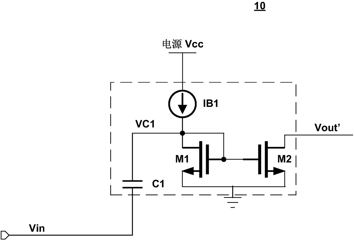
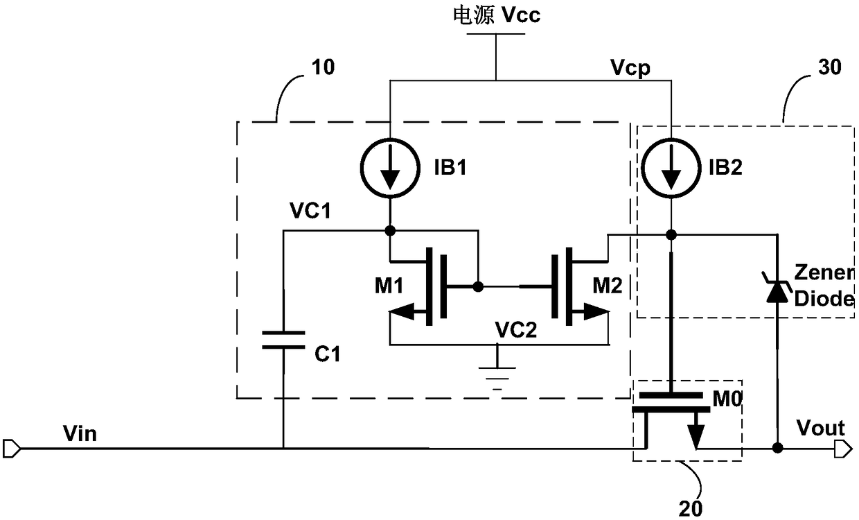
[0074] As mentioned in the background section, the off time of the load switch in the prior art is long and the response is slow. Even if there is a load switch with a fast response in the prior art, t...
PUM
 Abstract
Description
Claims
Application Information