A manufacturing method of an economical high-precision surface-enhanced Raman active substrate based on high-dielectric materials

A surface-enhanced Raman and manufacturing method technology, applied in the field of physical and chemical detection, can solve the problems of complicated preparation process, high cost, enhanced enhancement effect, etc., and achieve improved process reliability and stability, regular structure, and orderly arrangement. Effect

Inactive Publication Date: 2021-01-01
JIANGXI NORMAL UNIV
View PDF4 Cites 0 Cited by
  • Summary
  • Abstract
  • Description
  • Claims
  • Application Information

AI Technical Summary

Problems solved by technology

By adsorbing noble metal nanoparticles or self-assembled noble metal nanoparticles on the dielectric sphere array or self-assembling noble metal nanoparticles on the noble metal-covered dielectric sphere array, the intensity of the Raman signal of the molecules adsorbed on these structures can be compared with that of Compared with the noble metal thin film, it has been improved to a great extent, but the above structure still has the disadvantages of high cost, complicated preparation process, and the enhancement effect needs to be strengthened.

Method used


Image

  • A manufacturing method of an economical high-precision surface-enhanced Raman active substrate based on high-dielectric materials
  • A manufacturing method of an economical high-precision surface-enhanced Raman active substrate based on high-dielectric materials
  • A manufacturing method of an economical high-precision surface-enhanced Raman active substrate based on high-dielectric materials

Examples


Embodiment 1

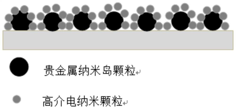
[0024] A method for manufacturing an economical high-precision surface-enhanced Raman active substrate based on high-dielectric materials, comprising the following steps:

[0025] (1) Preparation of noble metal nano-islands

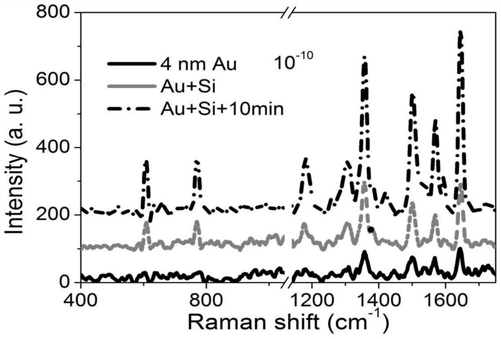
[0026] ① Use magnetron sputtering equipment to sputter the precious metal target onto the surface of clean quartz glass to form an ultra-thin nano-film layer of noble metal on the surface of quartz glass. The magnetron sputtering speed is controlled at 32nm / min, and the sputtering time is 7.6 seconds, the actual thickness of the noble metal nano-film layer is 4nm, where the noble metal target is a gold target;

[0027] ②Put the prepared noble metal nano-film layer into a muffle furnace and anneal at 200°C for 30 minutes to obtain a noble metal nano-island structure;

[0028] (2) Deposition of high dielectric nanoparticle materials

[0029] ① Use magnetron sputtering equipment to sputter the high dielectric target onto the surface of the noble metal nano...

Embodiment 2

[0037] A method for manufacturing an economical high-precision surface-enhanced Raman active substrate based on high-dielectric materials, comprising the following steps:

[0038] (1) Preparation of noble metal nano-islands

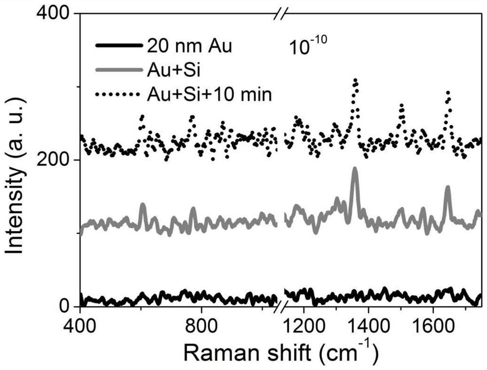
[0039] ①Use magnetron sputtering equipment to sputter noble metal target (gold target) onto the surface of clean quartz glass to form an ultra-thin noble metal nano-film layer on the surface of quartz glass. The magnetron sputtering speed is controlled at 32nm / min. The sputtering time is 38 seconds, and the actual thickness of the noble metal nano-film layer is 20nm;

[0040] ②Put the prepared noble metal nano-film layer into a muffle furnace and anneal at 200°C for 30 minutes to obtain a noble metal nano-island structure;

[0041] (2) Deposition of high dielectric nanoparticle materials

[0042] ①Use magnetron sputtering equipment to sputter the high dielectric target (silicon target) onto the surface of the noble metal nano-island structure prepared i...

Embodiment 3

[0050] A method for manufacturing an economical high-precision surface-enhanced Raman active substrate based on high-dielectric materials, comprising the following steps:

[0051] (1) Preparation of noble metal nano-islands

[0052] ①Use magnetron sputtering equipment to sputter noble metal target (gold target) onto the surface of clean quartz glass to form an ultra-thin noble metal nano-film layer on the surface of quartz glass. The magnetron sputtering speed is controlled at 32nm / min. The sputtering time is 3.8 seconds, and the actual thickness of the noble metal nano-film layer is 2nm;

[0053] ②Put the prepared noble metal nano-film layer into a muffle furnace and anneal at 200°C for 30 minutes to obtain a noble metal nano-island structure;

[0054] (2) Deposition of high dielectric nanoparticle materials

[0055] ①Use magnetron sputtering equipment to sputter the high dielectric target (silicon target) onto the surface of the noble metal nano-island structure prepared i...


PUM

PropertyMeasurementUnit
thicknessaaaaaaaaaa
thicknessaaaaaaaaaa
thicknessaaaaaaaaaa

Abstract

The invention relates to a manufacturing method of an economical high-precision surface-enhanced Raman active substrate based on high-dielectric materials, including the preparation of noble metal nano-islands, the deposition of high-dielectric nano-materials, HF and H 2 o 2 Three steps such as steam etching of the mixed solution, artificially controlling the scale of the noble metal nano-islands by magnetron sputtering and annealing, and then depositing high dielectric nanomaterials on the noble metal nano-islands by simple magnetron sputtering coating method, and then Take HF and H 2 o 2 The vapor of the mixed solution etches the sample to finally obtain. The method of the invention has good economy, high degree of standardization, strong Raman enhancement ability and identification ability, high reliability and good stability.

Description

technical field [0001] The invention relates to the field of physical and chemical detection, in particular to a method for manufacturing an economical high-precision surface-enhanced Raman active substrate of high dielectric material. Background technique [0002] The excitation of surface plasmons induced by noble metal nanostructures can provide strong Raman enhancement. Based on this characteristic of noble metal nanostructures, many surface-enhanced Raman scattering substrates have been developed. For example, the local surface enhancement effect based on discretized noble metal nanoparticles can achieve strong Raman enhancement, but the repeatability needs to be improved. The substrate structure prepared by complex methods such as focused ion beam etching, electron beam etching or template etching has a regular and ordered structure, and the Raman enhancement effect is very significant and repeatable, but the preparation cost is high and the instrument operation is com...

Claims


Application Information

Patent Timeline
Patent Type & Authority Patents(China)
IPC IPC(8): C23C14/18C23C14/06C23C14/08C23C14/35C23C14/58G01N21/65
CPCC23C14/0617C23C14/083C23C14/185C23C14/35C23C14/5806C23C14/5873G01N21/65G01N21/658G01N2021/655
Inventor 陈检刘桂强汤莉刘怡黄镇平
Owner JIANGXI NORMAL UNIV
Why Eureka
Try Eureka