Semiconductor structure and forming method thereof

A technology of semiconductor and gate structure, applied in the field of semiconductor structure and its formation, can solve problems such as the need to improve electrical performance, and achieve the effect of good electrical connection performance

Active Publication Date: 2018-10-16
SEMICON MFG INT (SHANGHAI) CORP +1
View PDF5 Cites 2 Cited by
  • Summary
  • Abstract
  • Description
  • Claims
  • Application Information

AI Technical Summary

Problems solved by technology

[0004] However, the electrical performance of the semiconductor structure with conductive plugs formed by the prior art needs to be improved

Method used


Image

  • Semiconductor structure and forming method thereof
  • Semiconductor structure and forming method thereof
  • Semiconductor structure and forming method thereof

Examples


Embodiment Construction

[0032] It can be seen from the background art that the electrical performance of the semiconductor structure with conductive plugs formed in the prior art needs to be improved.

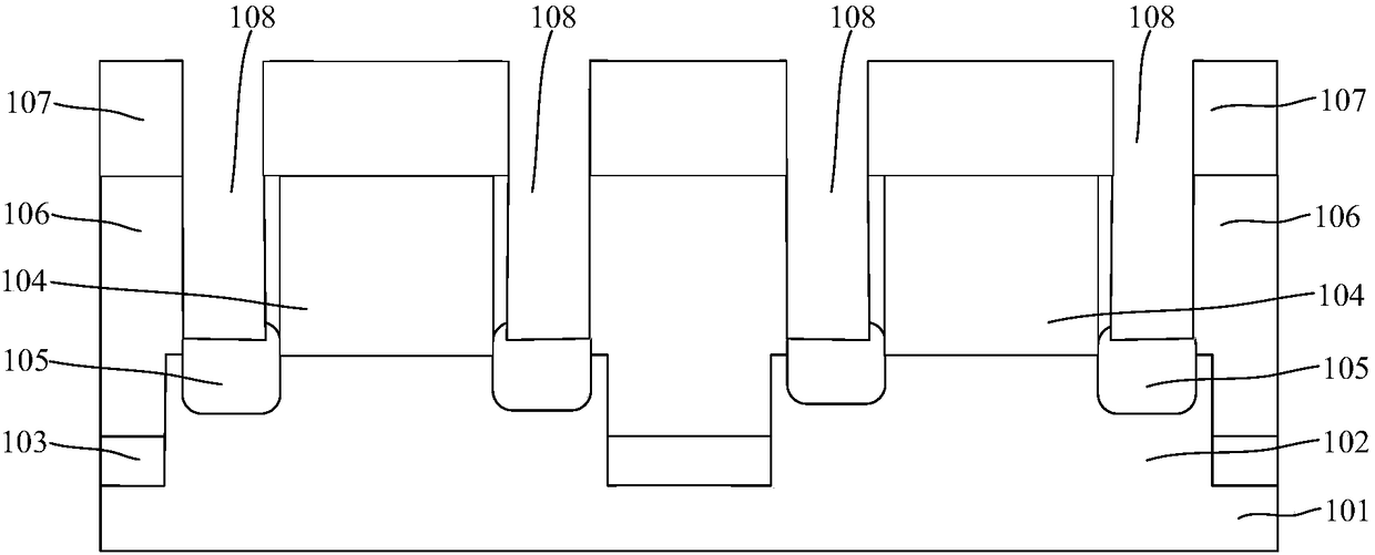
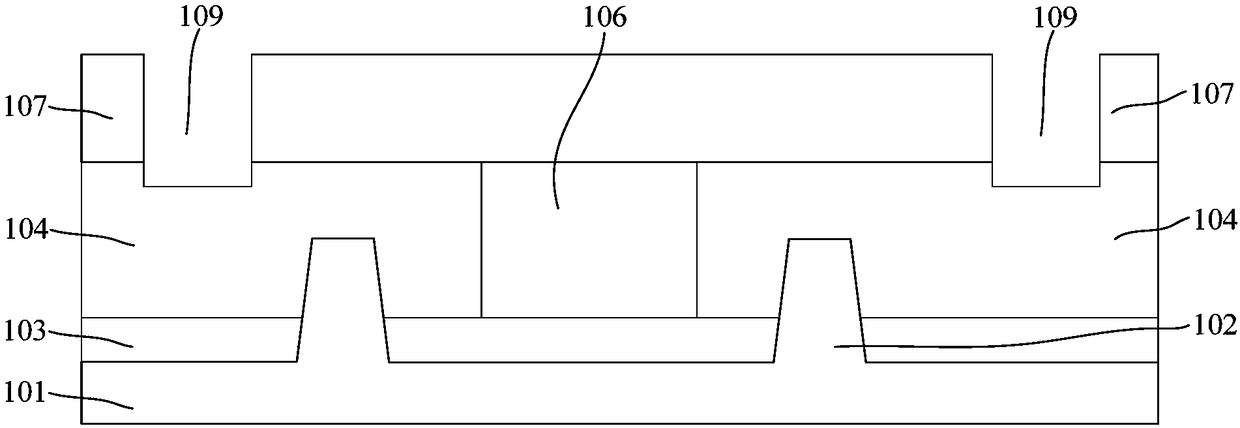
[0033] Now combine with a method of forming a semiconductor structure for analysis, refer to figure 1 and figure 2 ,in, figure 1 is a schematic diagram of a cross-sectional structure of a semiconductor structure along a direction parallel to the extension of the fin, figure 2 It is a schematic cross-sectional structure diagram of a semiconductor structure along the direction perpendicular to the extending direction of the fin.

[0034] refer to figure 1 and figure 2 , providing a substrate, the substrate has a gate structure 104, the substrate on both sides of the gate structure has source and drain doped regions 105, and the dielectric on the substrate exposed by the gate structure and on the top of the gate structure layer; through the first through hole 108 of the dielectric layer above the...


PUM

PropertyMeasurementUnit
thicknessaaaaaaaaaa

Abstract

The invention discloses a semiconductor structure and a forming method thereof. The forming method comprises the following steps of: forming a first through hole that penetrates through a dielectric layer and exposes a surface of a source-drain doping region; forming a second through hole that penetrates through the dielectric layer and exposes a top of a gate structure; depositing cap layers on abottom and sidewalls of the first through hole and a bottom and sidewalls of the second through hole; performing a first cleaning process on the bottom of the first through hole and the bottom of thesecond through hole to remove cap layers located on the bottom of the first through hole and the bottom of the second through hole; performing a second cleaning process on the source-drain doping region exposed at the bottom of the first through hole and the gate structure exposed at the bottom of the second through hole after the first cleaning process; forming metal layers on the bottom and thesidewalls of the first through hole, the bottom and the sidewalls of the second through hole and a top of the dielectric layer after the second cleaning process; and performing an annealing process on the metal layers to convert the metal layer located on the source-drain doping region into a metal silicide layer. According to the invention, the electrical properties of the formed semiconductor structure can be improved.

Description

technical field [0001] The invention relates to the technical field of semiconductor manufacturing, in particular to a semiconductor structure and a forming method thereof. Background technique [0002] As the production of integrated circuits develops towards ultra-large-scale integrated circuits, the circuit density inside integrated circuits is increasing, and the number of components contained is also increasing, making it difficult for the surface of the wafer to provide enough area to manufacture the required interconnections. connection. [0003] In order to meet the requirements of the interconnection line after the size of the component is reduced, the design of the interconnection metal layer has become a method usually adopted in the VLSI technology. At present, the conduction between the interconnected metal layers is realized through conductive plugs, and the conduction between the interconnected metal layers and the semiconductor structure is also realized thr...

Claims


Application Information

Patent Timeline
Patent Type & Authority Applications(China)
IPC IPC(8): H01L21/786H01L29/78H01L21/336
CPCH01L21/76879H01L21/76883H01L29/66795H01L29/785
Inventor 梁金娥
Owner SEMICON MFG INT (SHANGHAI) CORP
Why Eureka
Try Eureka