
Pulse semiconductor laser lighting system

A laser lighting and semiconductor technology, applied in the field of lighting, can solve the problems of limited application, low power of semiconductor lasers, human eye irritation, etc., and achieve the effect of improving system efficiency

Inactive Publication Date: 2018-10-19
HANGZHOU GUOYI TECH CO LTD +1
View PDF4 Cites 1 Cited by
  • Summary
  • Abstract
  • Description
  • Claims
  • Application Information

AI Technical Summary

Problems solved by technology

[0004] 1. Traditional lighting devices have high power consumption, low efficiency and are easy to cause glare
[0005] The luminous efficiency of traditional LED lighting devices is about 100Lm / W, which is nearly half lower than the luminous efficiency of semiconductor lasers of 190Lm / W
Secondly, in order to collect images of high-speed moving objects, its power consumption is sometimes as high as 100W or even 1kW
LED lighting devices exceeding 100W, because their emission spectrum is within the visible range of the human eye, can easily irritate the human eye, causing people to be temporarily dizzy and causing safety hazards
Although the solution of near-infrared semiconductor lasers can be used to prevent irritation to human eyes, the power consumption of continuous near-infrared semiconductor lasers is also high, resulting in low system efficiency
[0006] 2. Continuous semiconductor lasers have low power and limited applications
For example, when lighting a high-speed moving object, its optical power is required to exceed 100W or even hundreds of W. At this time, the heat generated is approximately equal to the output optical power, which is 100W or even hundreds of W. This is often unacceptable for system applications.
From this, it can be seen that the continuous laser will generate a lot of heat when it works, so as an illumination system, its power cannot be made too high, which greatly limits its application
The continuous semiconductor laser has low power, which limits its application; and its high power consumption leads to low system efficiency

Method used


Image

  • Pulse semiconductor laser lighting system
  • Pulse semiconductor laser lighting system
  • Pulse semiconductor laser lighting system

Examples


Embodiment Construction

[0027] Embodiments of the present invention are described in detail below, examples of which are shown in the drawings, wherein the same or similar reference numerals designate the same or similar elements or elements having the same or similar functions throughout. The embodiments described below by referring to the figures are exemplary only for explaining the present invention and should not be construed as limiting the present invention.

[0028] In the description of the present invention, unless otherwise specified and limited, it should be noted that the terms "installation", "connection" and "connection" should be understood in a broad sense, for example, it can be mechanical connection or electrical connection, or two The internal communication of each element may be directly connected or indirectly connected through an intermediary. Those skilled in the art can understand the specific meanings of the above terms according to specific situations.

[0029] Such as fig...


PUM


Abstract

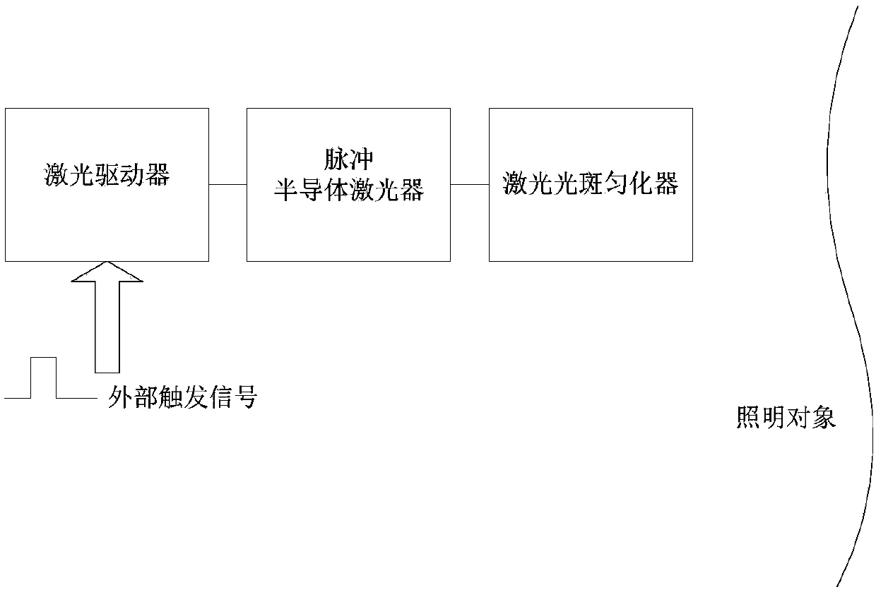
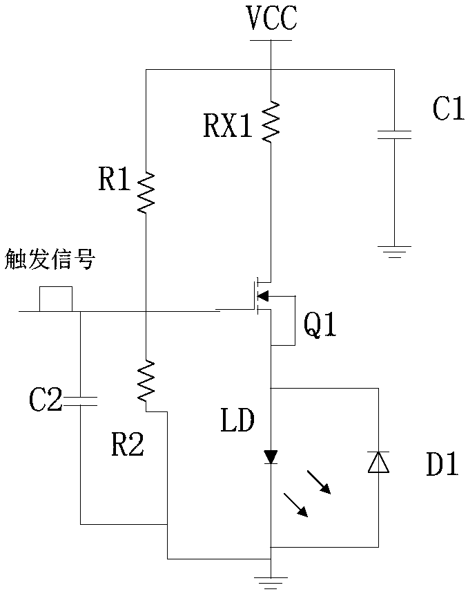
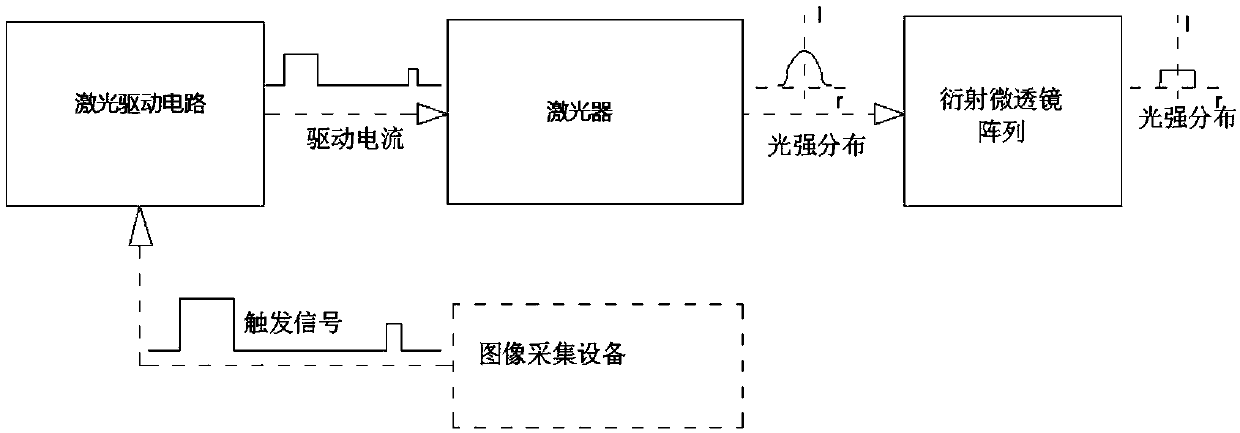
The invention relates to a pulse semiconductor laser lighting system as well as a lighting device used in a low-brightness area. The pulse semiconductor laser lighting system comprises a laser drivingcircuit, a pulse semiconductor laser and a laser spot homogenizer; the output end of the laser driving circuit is connected with the pulse semiconductor laser; the laser spot homogenizer is arrangedin front of light beams emitted by the pulse semiconductor laser; and the light beams emitted by the pulse semiconductor layer penetrate through the laser spot homogenizer. According to the laser lighting system, the system efficiency is improved, the system power consumption is reduced and high-power laser lighting application becomes possible.

Description

technical field [0001] The invention relates to the lighting field, in particular to a pulsed semiconductor laser lighting system and a lighting device used in a low-brightness area. Background technique [0002] With the continuous development of CCD and CMOS technology, image processing and video technology have been widely used. Since both CCD and CMOS are photoelectric sensing devices, in order to obtain clear image materials, both need to obtain sufficient exposure. At present, CCD or CMOS supplementary light sources are mostly LEDs and continuous semiconductor lasers. [0003] However, there are two major difficulties in traditional lighting installations: [0004] 1. Traditional lighting devices have high power consumption, low efficiency and are easy to cause glare [0005] The luminous efficiency of traditional LED lighting devices is about 100Lm / W, which is nearly half lower than the luminous efficiency of semiconductor lasers of 190Lm / W. Secondly, in order to ...

Claims


Application Information

Patent Timeline
IPC IPC(8): H01S5/042H01S5/00G02B27/09
CPCH01S5/0428G02B27/0927G02B27/0961H01S5/005
Inventor 彭涛武李祥邹泽亚苏力武同陆少刚
Owner HANGZHOU GUOYI TECH CO LTD
Learn More