Array substrate, manufacturing method thereof and display device

A technology for array substrates and display devices, which is applied to instruments, semiconductor devices, optics, etc., can solve the problems of signal wire lead wiring congestion and other problems, and achieve the effects of alleviating wiring congestion, reducing short-circuit risks, and avoiding open-circuit risks.

Inactive Publication Date: 2018-11-02
BOE TECH GRP CO LTD +1
View PDF8 Cites 16 Cited by
  • Summary
  • Abstract
  • Description
  • Claims
  • Application Information

AI Technical Summary

Problems solved by technology

[0005] Embodiments of the present invention provide an array substrate, a manufacturing method thereof, and a display device, so as to alleviate the problem of overcrowded wiring of signal lines in the prior art

Method used


Image

  • Array substrate, manufacturing method thereof and display device
  • Array substrate, manufacturing method thereof and display device
  • Array substrate, manufacturing method thereof and display device

Examples


Embodiment Construction

[0043] In order to make the object, technical solution and advantages of the present invention clearer, the implementation manner of the present invention will be further described in detail below in conjunction with the accompanying drawings.

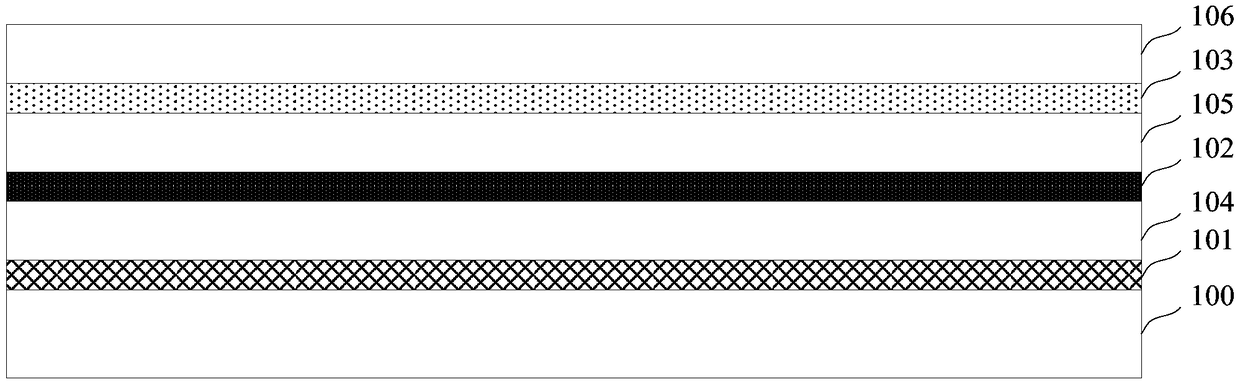
[0044] figure 1 It is a schematic structural diagram of an array substrate provided by an embodiment of the present invention, the array substrate includes a substrate 100, and a first metal layer 101, a second metal layer 102, and a third metal layer 103 disposed on the substrate 100, The first metal layer 101 , the second metal layer 102 and the third metal layer 103 are insulated from each other.

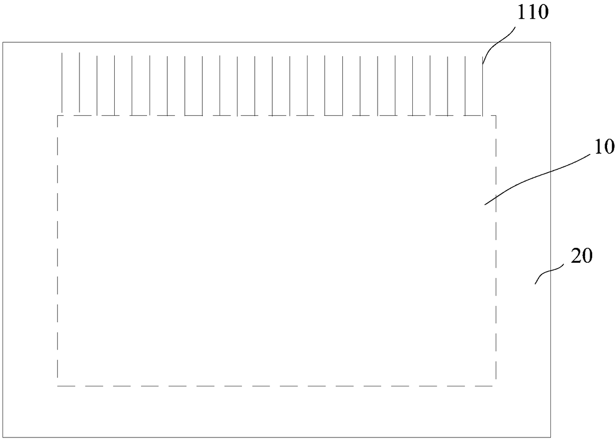
[0045] figure 2 is a top view of the array substrate provided by the embodiment of the present invention, see figure 2, the array substrate is divided into a display area 10 and a peripheral area 20 ; the peripheral area 20 of the array substrate is provided with a plurality of signal wire leads 110 . A part of the plurality of signa...


PUM


Abstract

The invention discloses an array substrate, a manufacturing method thereof and a display device, and belongs to the field of display. The array substrate includes a substrate, a first metal layer, a second metal layer, and a third metal layer, wherein the first metal layer, the second metal layer and the third metal layer are disposed on the substrate; the array substrate is divided into a displayarea and a peripheral area; the peripheral area of the array substrate is provided with a plurality of signal line leads, one part of the plurality of signal line leads are located at the first metallayer, another part of the plurality of signal line leads are located in at least one layer of the third metal layer and the second metal layer, the first metal layer includes a shading layer locatedat the display area, the second metal layer comprises a gate layer located at the display area, and the third metal layer includes a source and drain layer located at the display area. In the case where the peripheral area is small, the wiring congestion of the signal line leads is alleviated, the signal line lead pitch is increased, a short circuit risk is lowered, and the signal line leads canbe designed to be thicker due to the reduced wiring congestion, thereby avoiding the open circuit risk of the signal line leads.

Description

technical field [0001] The invention relates to the field of displays, in particular to an array substrate, a manufacturing method thereof, and a display device. Background technique [0002] With the development of liquid crystal displays, products with high PPI (Pixels Per Inch, pixels per inch), high resolution, and high screen-to-body ratio are favored by more and more consumers. [0003] However, with the continuous improvement of PPI, resolution, and screen-to-body ratio, the number of signal lines (such as data lines and gate lines) in the display area of ​​the liquid crystal display will increase. Correspondingly, the number of signal wire leads located in the peripheral area (or fan-out (Fan-out) area) of the liquid crystal display screen will also increase. The function of the signal wire leads is to connect the signal wires to the integrated circuit. [0004] Among them, the signal line leads are arranged in the source and drain layers of the peripheral area. Due...

Claims


Application Information

Patent Timeline
Patent Type & Authority Applications(China)
IPC IPC(8): G02F1/1362G02F1/1343
CPCG02F1/134309G02F1/136286G02F1/13629H01L27/124G02F1/13458H01L27/1237H01L27/1259H01L27/1244
Inventor 张文龙张绪张伟田建飞徐敬义韩帅
Owner BOE TECH GRP CO LTD
Why Eureka
Try Eureka