Drain leakage current testing circuit and method in field effect transistor breakdown voltage characteristic
A field effect transistor and breakdown voltage technology, applied in the direction of testing dielectric strength, measuring electricity, measuring devices, etc., can solve the problems of high price, inability to guarantee measurement accuracy, non-compliance, etc., to save hardware costs and improve test accuracy. And the effect of high efficiency and high test accuracy
- Summary
- Abstract
- Description
- Claims
- Application Information
AI Technical Summary
Problems solved by technology
Method used
Image

Examples
Embodiment 1
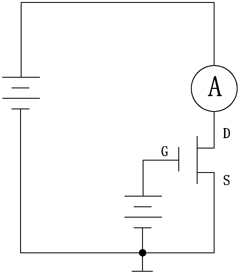
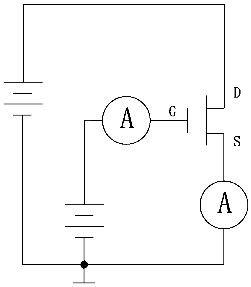
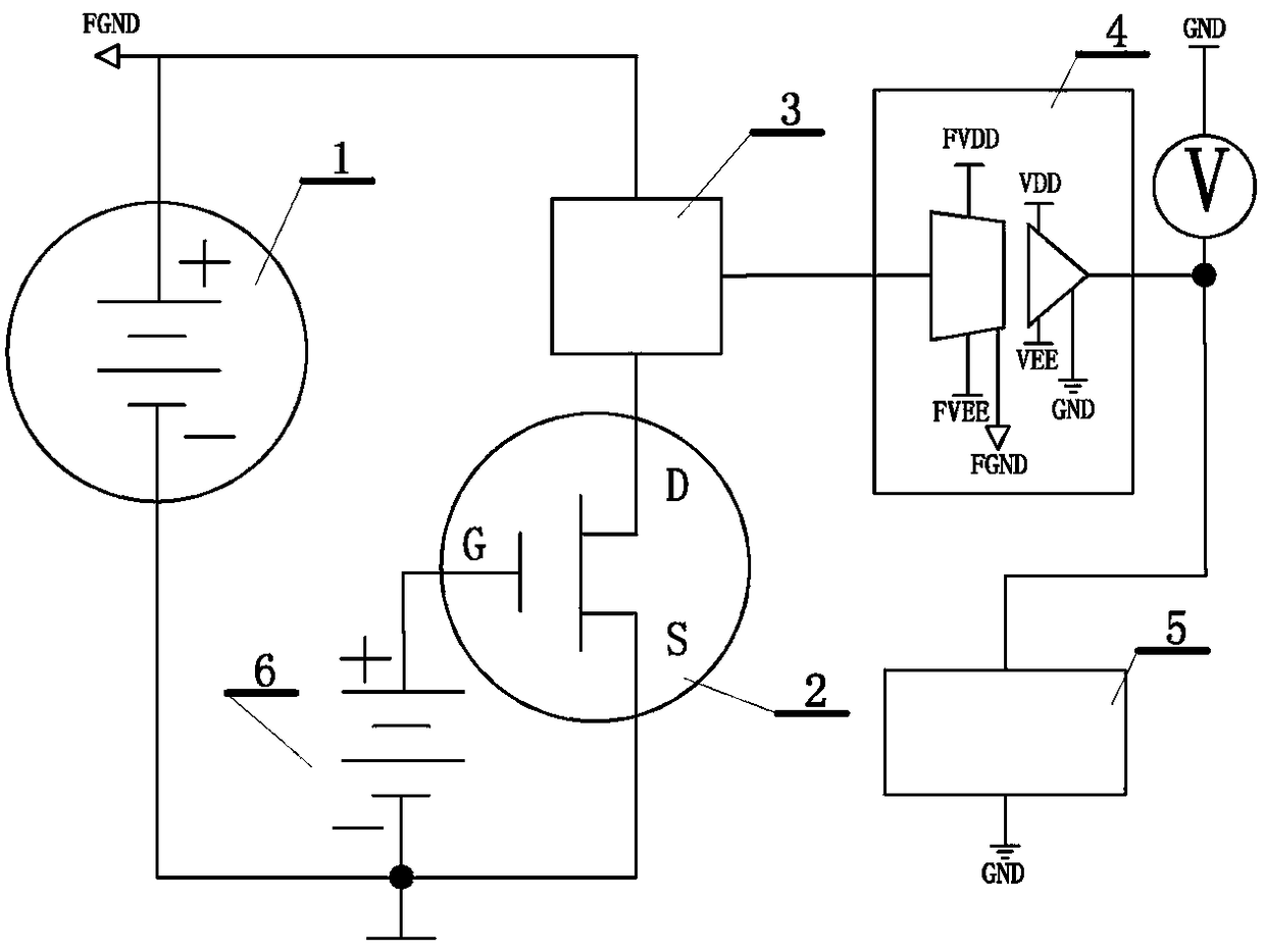
[0031] A drain leakage current test circuit in the field effect transistor breakdown voltage characteristics, such as image 3 As shown, the drain leakage current test circuit includes a test voltage source 1 and a field effect transistor under test 2, and the test voltage source is used to apply a voltage to the drain D and source S of the field effect transistor under test, wherein, during the test A current / voltage conversion amplification module 3 is arranged between the positive pole of the voltage source 1 and the drain D of the field effect transistor, and the voltage output signal of the current / voltage conversion amplification module is transmitted to a signal input terminal of an isolation amplifier module 4, and the current The / voltage conversion amplification module is to obtain the sampling resistance signal by an operational amplifier to form a current / voltage conversion, and the isolation output of the isolation amplifier module is connected to a microprocessor ...
Embodiment 2
[0040] A drain leakage current testing method in field effect transistor breakdown voltage characteristics is based on the testing method of the drain leakage current testing circuit in embodiment 1, so the content in embodiment 1 should be the content in this embodiment. Therefore, the test circuit includes a test voltage source and a measured field effect transistor, the test voltage source is used to apply a voltage to the drain D and the source S of the tested field effect transistor, and the positive electrode of the test voltage source and the field effect transistor drain A current / voltage conversion amplification module is arranged between the poles D, and the voltage output signal of the current / voltage conversion amplification module is transmitted to the input terminal of an isolation amplifier module. The current / voltage conversion amplification module is composed of an operational amplifier and a sampling resistor. The isolation output terminal of the isolation amp...
PUM
 Abstract
Description
Claims
Application Information
 - Generate Ideas
- Intellectual Property
- Life Sciences
- Materials
- Tech Scout
- Unparalleled Data Quality
- Higher Quality Content
- 60% Fewer Hallucinations
Browse by: Latest US Patents, China's latest patents, Technical Efficacy Thesaurus, Application Domain, Technology Topic, Popular Technical Reports.
© 2025 PatSnap. All rights reserved.Legal|Privacy policy|Modern Slavery Act Transparency Statement|Sitemap|About US| Contact US: help@patsnap.com