Liquid crystal display panel

A liquid crystal display panel and display area technology, applied in nonlinear optics, instruments, optics, etc., can solve problems such as poor bonding of drive chips, affecting display effects, and increased bonding impedance, so as to avoid the reduction of effective contact area , improve the display effect, and avoid the effect of bad bonding

Inactive Publication Date: 2018-11-06
WUHAN CHINA STAR OPTOELECTRONICS TECH CO LTD
View PDF4 Cites 15 Cited by
  • Summary
  • Abstract
  • Description
  • Claims
  • Application Information

AI Technical Summary

Problems solved by technology

[0006] like figure 1 and figure 2 As shown, it is a schematic diagram of an existing liquid crystal display panel, including: an adjacent display area 100 and a frame area 200, and the frame area 200 includes a base substrate 201 and a metal wiring layer 202 disposed on the base substrate 201 , a planar layer (PLN) 203 disposed on the metal wiring layer 202, an insulating layer 204 disposed on the planar layer 203, a bonding (bongding) terminal 205 disposed on the insulating layer 204, and a bonding terminal 205 disposed on The anisotropic conductive glue (ACF glue) 206, the driver chip (IC) connection terminal 207 on the ACF glue 206 and the PI alignment film 208 on the insulating layer 204; the flat layer 203 has a groove 209 , the bonding terminal 205 is formed in the groove 209 and contacts the metal wiring layer 202 through a via hole 210 penetrating the insulating layer 204; The fluidity of the bonding terminal 205 covers the bonding terminal 205, resulting in a decrease in the effective contact area between the driver chip connection terminal 207 and the bonding terminal 205, an increase in the bonding impedance, and even an open circuit, resulting in poor bonding of the driver chip and affecting the display. Effect

Method used


Image

  • Liquid crystal display panel
  • Liquid crystal display panel
  • Liquid crystal display panel

Examples


Embodiment Construction

[0028] In order to further illustrate the technical means adopted by the present invention and its effects, the following describes in detail in conjunction with preferred embodiments of the present invention and accompanying drawings.

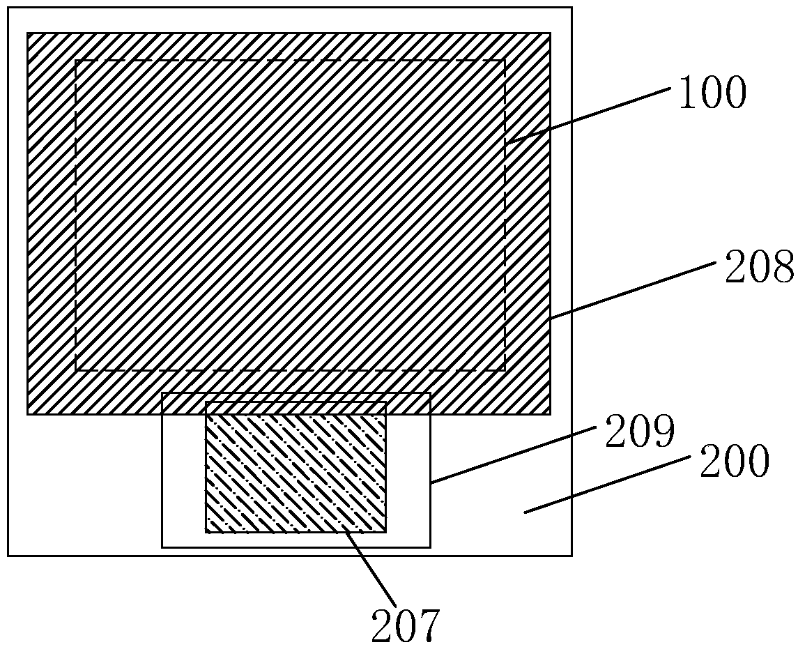
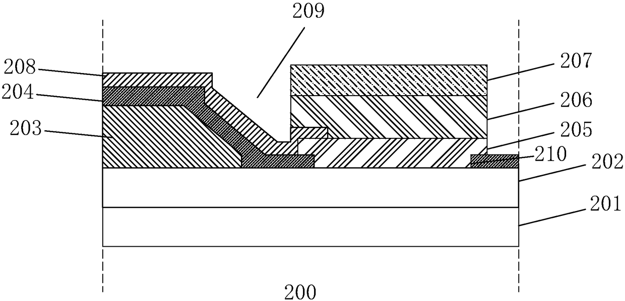
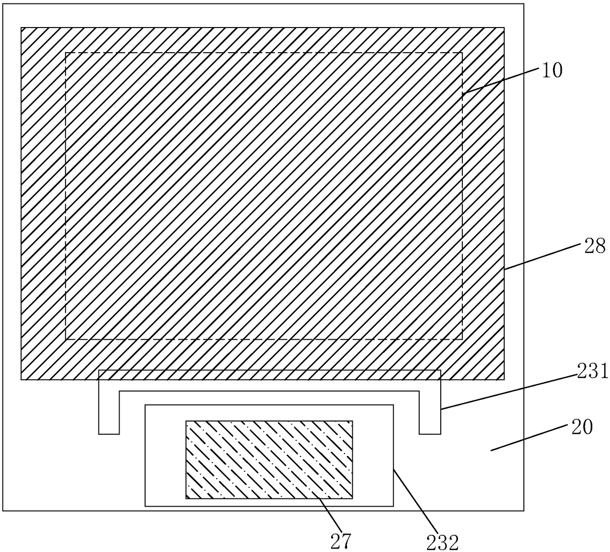
[0029] see image 3 and Figure 6 , the liquid crystal display panel of the present invention comprises: adjacent display area 10 and frame area 20; Said frame area 20 comprises base substrate 21, the metal wiring layer 22 that is arranged on the base substrate 21, is arranged on the metal wiring layer The flat layer 23 on the layer 22, the insulating layer 24 on the flat layer 23 and the metal wiring layer 22, the bonding terminal 25 on the insulating layer 24 and the metal wiring layer 22, and the bonding terminal 25 The anisotropic conductive adhesive 26, the connecting terminal 27 provided on the anisotropic conductive adhesive 26, and the alignment film 28 provided on the insulating layer 24;

[0030] At least one flow blocking groove 2...


PUM

PropertyMeasurementUnit
angleaaaaaaaaaa

Abstract

The invention provides a liquid crystal display panel. The liquid crystal display panel comprises a display area and a border area which are adjacent, the border area comprises an underlayer substrate, a metal wiring layer arranged on the underlayer substrate, a flat layer arranged on the metal wiring layer, an insulating layer arranged on the flat layer and the metal wiring layer, a bonding terminal arranged on the insulating layer and the metal wiring layer, an anisotropic conductive adhesive arranged on the bonding terminal, a connecting terminal arranged on the anisotropic conductive adhesive and an alignment film arranged on the insulating layer; at least one blocking groove is formed between the display area and the bonding terminal, the alignment film of the border area can only flow into the blocking grooves, the phenomenon that the alignment film covers the bonding terminal due to certain mobility is prevented, the phenomenon that the effective contact area of the connecting terminal and the bonding terminal is reduced is avoided, the phenomenon that liquid crystal display panel bonding is poor is avoided, the display effect is improved, and narrow bezel of the liquid crystal display panel is facilitated.

Description

technical field [0001] The invention relates to the field of display technology, in particular to a liquid crystal display panel. Background technique [0002] With the development of display technology, liquid crystal display (Liquid Crystal Display, LCD) has gradually replaced cathode ray tube (Cathode Ray Tube, CRT) display due to its advantages of high image quality, power saving, thin body and wide application range. , are widely used in various consumer electronic products such as mobile phones, televisions, personal digital assistants, digital cameras, notebook computers, and desktop computers, and become the mainstream of display devices. [0003] Most of the liquid crystal displays currently on the market are backlight liquid crystal displays, which include a liquid crystal display panel and a backlight module (Backlight Module). The working principle of the liquid crystal display panel is to pour liquid crystal molecules between the thin film transistor array subs...

Claims


Application Information

Patent Timeline
Patent Type & Authority Applications(China)
IPC IPC(8): G02F1/1345G02F1/1337
CPCG02F1/1337G02F1/13452
Inventor 李彦阳
Owner WUHAN CHINA STAR OPTOELECTRONICS TECH CO LTD
Why Eureka
Try Eureka