
Beam-film double island structure micro-pressure high-overload sensor chip

A sensor chip, high overload technology, applied in the direction of microstructure technology, microstructure devices, piezoelectric devices/electrostrictive devices, etc., can solve the problem that cannot meet the requirements of accurate measurement in the aerospace field and Pa-level micro-pressure measurement in the aerospace field needs, can not adapt to the working environment in the aerospace field and other issues

Inactive Publication Date: 2012-08-01
XI AN JIAOTONG UNIV
View PDF4 Cites 12 Cited by
  • Summary
  • Abstract
  • Description
  • Claims
  • Application Information

AI Technical Summary

Problems solved by technology

[0003] With the development of aerospace technology, my country's current MEMS micro-pressure sensors are still mainly at the KPa level, which cannot meet the needs of the aerospace field for Pa-level micro-pressure measurement, nor can it adapt to the working environment of the aerospace field, and cannot meet the needs of the aerospace field. Requirements for precise measurement technology of deep and high-altitude micro-pressure

Method used


Image

  • Beam-film double island structure micro-pressure high-overload sensor chip
  • Beam-film double island structure micro-pressure high-overload sensor chip
  • Beam-film double island structure micro-pressure high-overload sensor chip

Examples


Embodiment Construction

[0021] Embodiments of the present invention will be described in detail below in conjunction with the accompanying drawings.

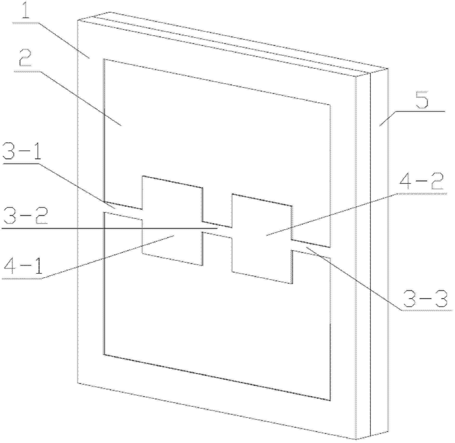
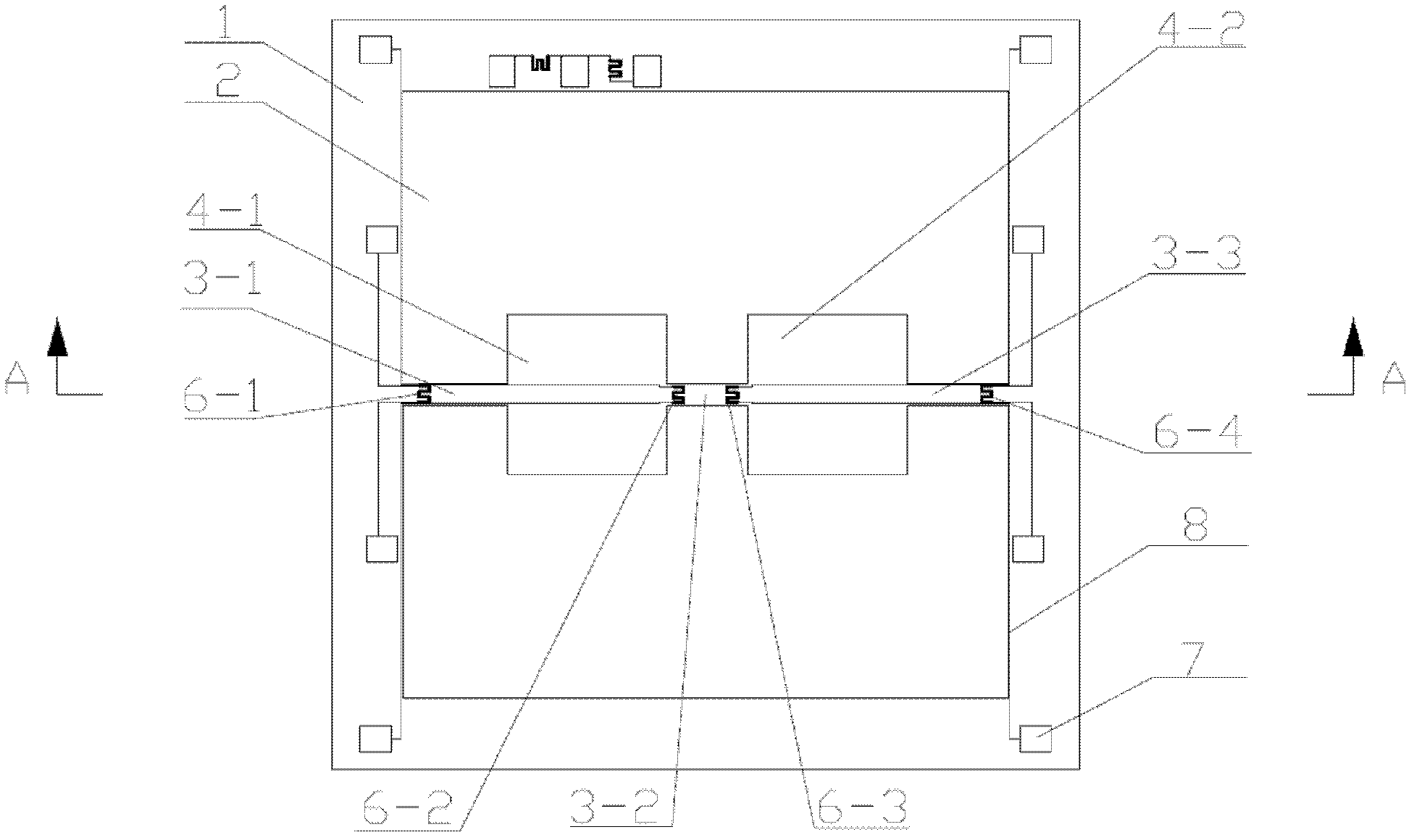
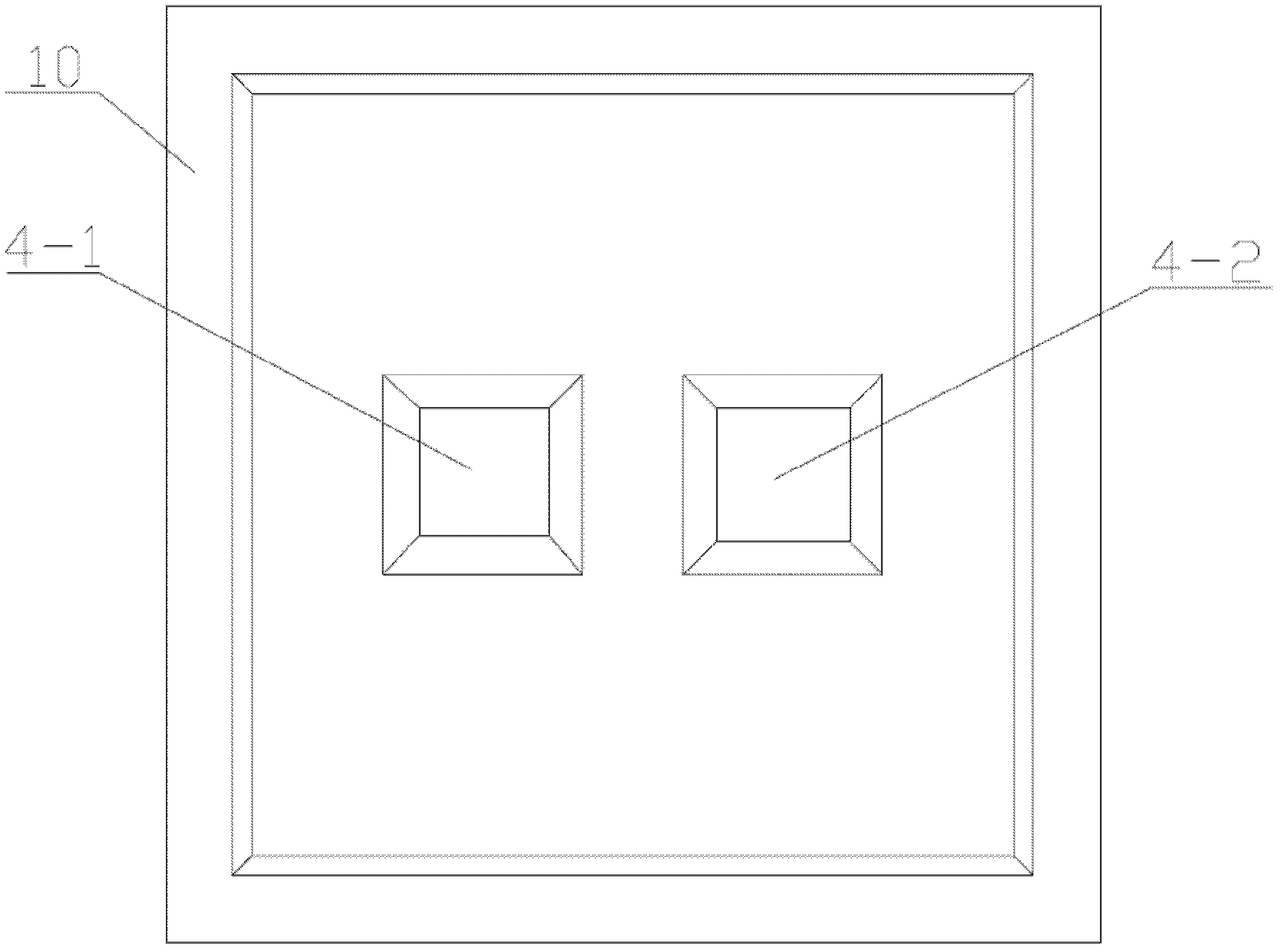
[0022] refer to figure 1 and figure 2 , a beam-membrane double-island structure micro-voltage high-overload sensor chip, comprising a silicon substrate 1 on which two mass blocks 4-1, 4-2 and three single beams 3-1, 3-2, 3 are processed -3, the first mass 4-1 is connected to the silicon substrate 1 through the first single beam 3-1, the second mass 4-2 is connected to the silicon substrate 1 through the third single beam 3-3, and the first mass 4 -1 and the second mass block 4-2 are connected through the second single beam 3-2, and the silicon substrate 1, mass blocks 4-1, 4-2 and three single beams 3-1, 3-2, 3- The space surrounded by 3 is processed into a thin film 2 of 10-30 μm, and the back side of the silicon substrate 1 is bonded to the Pyrex7740 glass 5, refer to image 3 , Figure 4 and Figure 5 , the back of the mass blocks 4-1, 4-2 is ...


PUM

PropertyMeasurementUnit
thicknessaaaaaaaaaa

Abstract

The invention relates to a beam-film double island structure micro-pressure high-overload sensor chip. The beam-film double island structure micro-pressure high-overload sensor chip comprises a silicon substrate, wherein two mass blocks and three single beams are processed on the silicon substrate; the single beams are connected between the mass blocks and the silicon substrate and between the two mass blocks; a spaced surrounded by the silicon substrate, the mass blocks and the three single beams is processed into a thin film; the rear surface of the silicon substrate is bonded with Pyrex7740 glass; gaps are formed between the mass blocks and the Pyrex7740 glass in vacuum environment; two anti-adsorbent electrodes on the Pyrex7740 glass are inserted into a bonding region; a cavity formed by the thin film, the mass blocks and the Pyrex7740 glass is vacuumized; and four piezoresistor stripes are mutually connected to form an open-loop wheatstone bridge on the front surface of the silicon substrate. The whole rigidity is improved by introducing the three single beams, and the stress is concentrated again. The beam-film double island structure micro-pressure high-overload sensor chip has the characteristics of high linearity, high sensitivity and low zero position and can resist 500 times of high overload at the same time.

Description

technical field [0001] The invention relates to the technical field of MEMS piezoresistive absolute pressure sensors, in particular to a beam-membrane double-island structure micro-pressure high-overload sensor chip. Background technique [0002] With the development of micro-mechanical electronic system technology, MEMS micro-pressure sensors have been widely used in wind tunnel testing, biomedical electronics, petrochemical and other fields, especially in aerospace, which has strict requirements on sensor volume and weight. MEMS Sensors are undoubtedly the ideal choice. [0003] With the development of aerospace technology, my country's current MEMS micro-pressure sensors are still mainly at the KPa level, which cannot meet the needs of the aerospace field for Pa-level micro-pressure measurement, nor can it adapt to the working environment of the aerospace field, and cannot meet the needs of the aerospace field. The demand for precise measurement technology of deep and hig...

Claims


Application Information

Patent Timeline
Patent Type & Authority Applications(China)
IPC IPC(8): G01L1/18B81B3/00B81B7/00
Inventor 赵玉龙于忠亮孟夏薇刘岩张学锋王伟忠
Owner XI AN JIAOTONG UNIV
Learn More