MEMS wafer level vacuum package structure and manufacturing method thereof

A technology of vacuum packaging and manufacturing method, applied in microstructure technology, microstructure device, manufacturing microstructure device, etc., can solve the problems of the vacuum degree of the inner cavity can not be maintained for a long time, the thermal expansion coefficient is inconsistent, and can not meet the high-end devices, etc. Avoid thermal stress, achieve small package size, and design flexibility

Inactive Publication Date: 2016-02-03
BEIJING MXTRONICS CORP +1
View PDF4 Cites 12 Cited by
  • Summary
  • Abstract
  • Description
  • Claims
  • Application Information

AI Technical Summary

Problems solved by technology

At present, wafer-level packaging is mostly used by anodic bonding process, that is, glass is used as a sealing cover to seal the silicon structure inside its cavity, but this method still has the following shortcomings: (1) due to the combination of glass and silicon The thermal expansion coefficients are inconsistent, resulting in a large temperature drift of the device, which seriously affects the performance of the device
(2) After the anodic bonding is completed, once the device is cut off, additional bonding wires are required for normal use, and the process is complicated
(3) The glass will release gas during the bonding process, resulting in the vacuum of the internal cavity cannot be maintained at a low pressure level for a long time, which cannot meet the needs of high-end devices

Method used


Image

  • MEMS wafer level vacuum package structure and manufacturing method thereof
  • MEMS wafer level vacuum package structure and manufacturing method thereof
  • MEMS wafer level vacuum package structure and manufacturing method thereof

Examples


Embodiment Construction

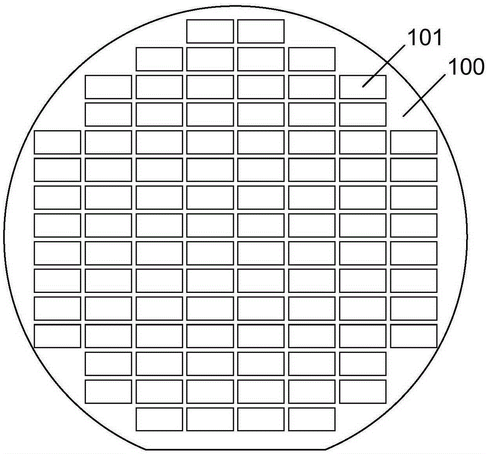
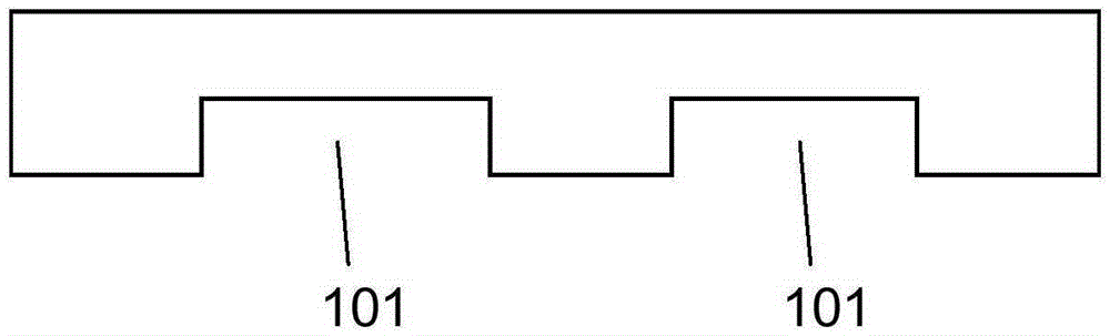
[0046]The present invention proposes a MEMS wafer-level vacuum packaging structure, including a silicon cover 100 and a MEMS wafer 200 with a movable structure 201; the silicon cover 100 is double-sided polished, and the lower surface of the silicon cover 100 is selected as the bonding surface , N grooves 101 for accommodating the movable structure 201 are processed on the bonding surface, and the bottom of the grooves 101 is covered with a layer of getter film; The conductive material 104 made of Cu or Au is filled in the hole 102, and the two ends of the conductive material 104 are respectively flush with the upper and lower surfaces of the silicon cover plate 100; The area other than the groove 101 and the upper surface of the silicon cover plate 100 are all provided with an insulating layer 103, and the material of the insulating layer is SiO 2 or Si 3 N 4 A metal bonding region 105 made of a single-layer or multi-layer AuSn metal thin film material is processed on the i...


PUM

PropertyMeasurementUnit
thicknessaaaaaaaaaa
diameteraaaaaaaaaa
electrical resistivityaaaaaaaaaa

Abstract

The invention provides an MEMS wafer level vacuum package structure and a manufacturing method thereof. The package structure comprises a silicon cover plate and an MEMS wafer with a movable structure, wherein a vertical through hole is formed on the cover plate, the through hole is internally filled with a conductive material, a bonding surface of the cover plate is provided with a groove, a layer of getter film is arranged at the bottom of the groove, and the silicon cover plate and the MEMS wafer with the movable structure form the vacuum package structure by wafer bonding. The manufacturing method provided by the invention comprises the following steps: at first, manufacturing the through hole on the cover plate, and filling the conductive material in the hole; and then, forming the groove on the bonding surface, depositing a layer of getter film on the bottom of the groove, depositing a layer of multilayer metal film in a bonding area, and wafer bonding the cover plate with the MEMS wafer with the movable structure in a vacuum environment. According to the MEMS wafer level vacuum package structure provided by the invention, the groove with the getter and the through hole are formed on the silicon cover plate to export an electrode from the closed groove without carrying out wire bonding, so that the procedures are simple, meanwhile, the vacuum maintenance ability in the package structure is improved, contamination of granules to the movable structure during cutting is avoided, and performance of the device is guaranteed.

Description

technical field [0001] The invention relates to a MEMS wafer-level vacuum packaging structure and a manufacturing method thereof, which are applied in the field of MEMS sensor packaging. Background technique [0002] For MEMS resonant devices such as gyroscopes, accelerometers, and resonators, it is especially important to work in a vacuum airtight environment, such as under a standard atmospheric pressure, affected by air damping, the driving mode and sensitive mode of silicon micro MEMS gyroscopes The quality factor is very low (the Q value is generally less than 500), and the Q value can reach 50,000 in a vacuum environment, and the performance is several orders of magnitude different. Therefore, resonant devices such as silicon micro MEMS gyroscopes maintain stable resonant frequency and gas damping coefficient in a vacuum environment to ensure good working performance. [0003] In China, device-level vacuum packaging is generally used to meet the needs of the above-men...

Claims


Application Information

Patent Timeline
Patent Type & Authority Applications(China)
IPC IPC(8): B81B3/00B81B7/00B81C1/00B81C3/00
Inventor 张富强杨静孟美玉李光北孙俊敏钟立志
Owner BEIJING MXTRONICS CORP
Why Eureka
Try Eureka