Method for detecting flatness of wafer table

A workbench and flatness technology, applied in the direction of measuring devices, semiconductor/solid-state device testing/measurement, instruments, etc., can solve the problems of untimely detection, loss of wafer yield, and flatness detection of the edge of the wafer workbench Major and other issues

Active Publication Date: 2018-11-06
SHANGHAI HUALI MICROELECTRONICS CORP
View PDF10 Cites 3 Cited by
  • Summary
  • Abstract
  • Description
  • Claims
  • Application Information

AI Technical Summary

Problems solved by technology

However, due to factors such as the focus failure range and the size of the flatness test device, it is difficult to detect the flatness of the edge of the wafer table.
Moreover, the edge area of ​​the wafer table is more likely to accumulate particles, because the abnormality of the flatness of the edge of the wafer table cannot be detected in time, which will cause the yield loss of the wafers at the edge of the wafer table

Method used


Image

  • Method for detecting flatness of wafer table

Examples


Embodiment Construction

[0026] The specific implementation manner of the present invention will be described in more detail below with reference to schematic diagrams. Advantages and features of the present invention will be apparent from the following description and claims. It should be noted that all the drawings are in a very simplified form and use imprecise scales, and are only used to facilitate and clearly assist the purpose of illustrating the embodiments of the present invention.

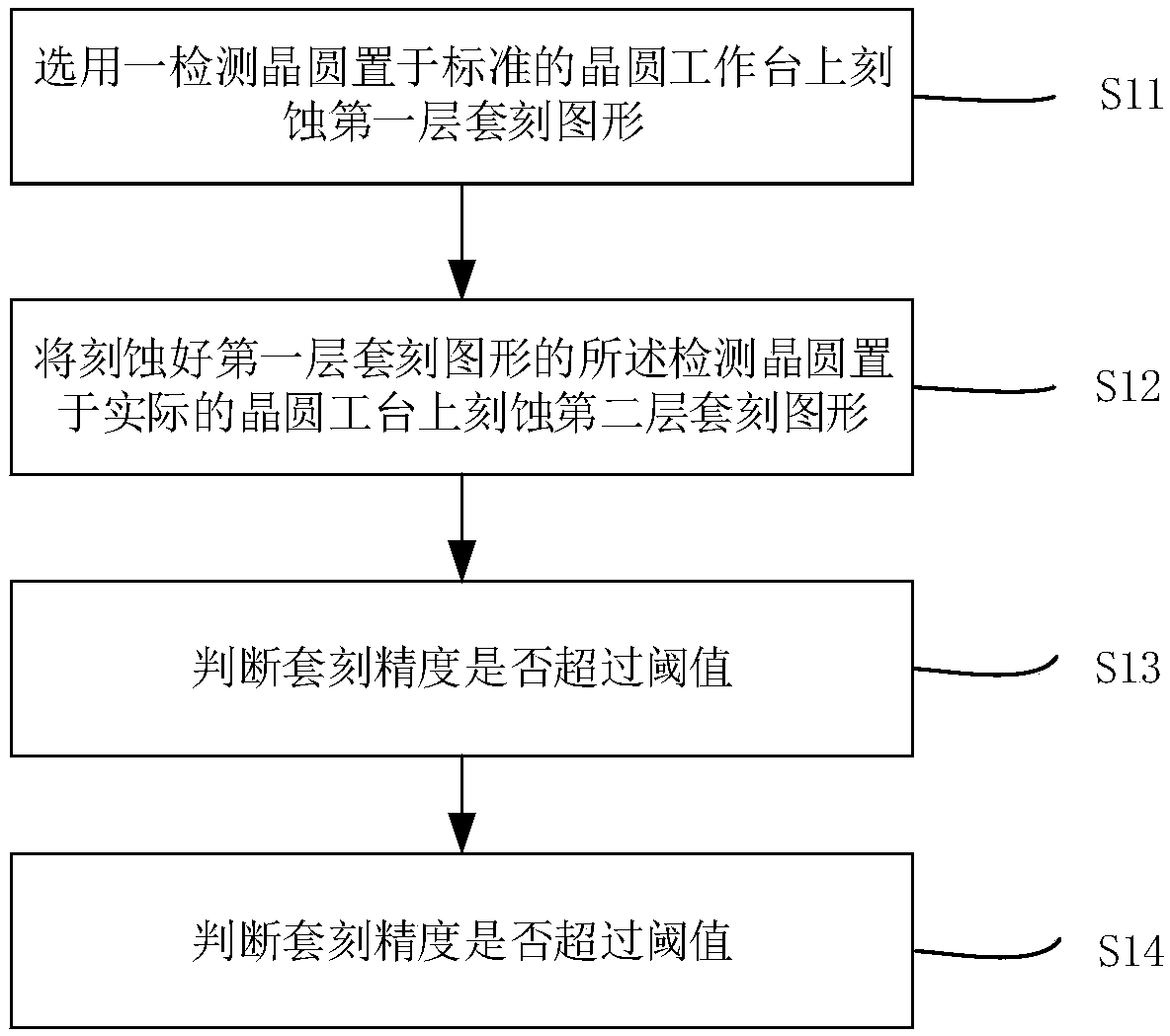
[0027] refer to figure 1 , the invention provides a method for detecting the flatness of a wafer workbench, comprising:

[0028] S11: selecting a test wafer and placing it on a standard wafer workbench to etch the first layer of overlay patterns;

[0029] S12: placing the test wafer with the etched first-layer overlay pattern on an actual wafer workbench to etch the second-layer overlay pattern;

[0030] S13: Calculate the overlay accuracy of the second layer of overlay graphics relative to the first layer of ...


PUM


Abstract

The invention provides a method for detecting the flatness of a wafer table. The method comprises the steps of putting a selected detection wafer on a standard wafer table and etching a first layer ofnesting graphics; putting the detection wafer etched with the first layer of nesting graphics on an actual wafer table and etching a second layer of nesting graphics; calculating the nesting accuracyof the second layer of nesting graphics relative to the first layer of nesting graphics; and comparing the calculated nesting accuracy with a threshold, and if the nesting accuracy exceeds the threshold, judging that the flatness of the wafer table does not reach a standard value. According to the method for detecting the flatness of the wafer table provided by the invention, the value of the nesting accuracy is calculated and recorded through measuring the nesting accuracy of the wafer, and whether the wafer table needs to be cleaned or not is judged through judging whether the nesting accuracy exceeds the threshold or not. According to the method, the flatness of the wafer table can be detected, so that the probability of a bad wafer caused by the flatness is finally reduced.

Description

technical field [0001] The invention relates to the technical field of integrated circuit manufacturing, in particular to a method for detecting the flatness of a wafer workbench. Background technique [0002] The flatness of the wafer table in the lithography machine directly affects the exposure results. If the flatness is not good, it will lead to poor graphics focus, resulting in defects and yield loss. In the prior art, the abnormality of the flatness of the wafer workbench can be found in time by using the flatness detection element. However, due to the thickness of the glue-coated film on the edge of the wafer, and the settings of edge washing and edge removal, the failure range of the lithography machine is usually defined as 3mm, and a chip with a radius of 150mm is used as an example. The radius is within 14mm, and the failure range is outside 14mm. However, due to factors such as the focus failure range and the size of the flatness test device, it is difficult t...

Claims


Application Information

Patent Timeline
Patent Type & Authority Applications(China)
IPC IPC(8): H01L21/66G01B21/30
CPCG01B21/30H01L22/12
Inventor 刘小虎朱祎明
Owner SHANGHAI HUALI MICROELECTRONICS CORP
Why Eureka
Try Eureka