IP core for realizing Powerlink industrial real-time Ethernet communication
An Ethernet, industrial technology, applied in the direction of bus network, data exchange network, data exchange through path configuration, etc., can solve the problems of unstable transmission, slow communication response, high communication cost, etc.
- Summary
- Abstract
- Description
- Claims
- Application Information
AI Technical Summary
Problems solved by technology
Method used
Image
Examples
Embodiment 1
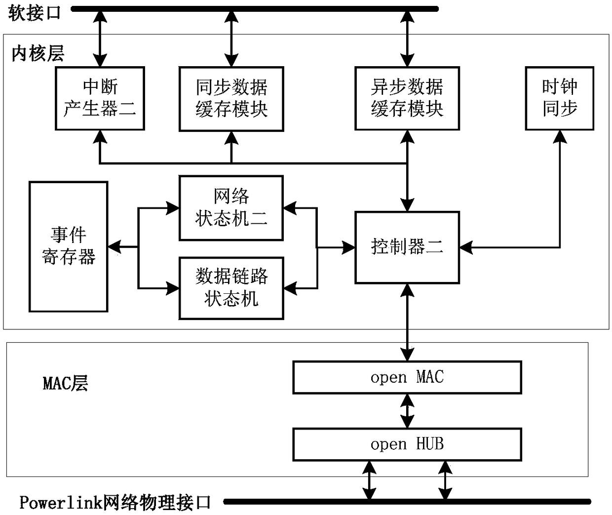
[0037] The IP core of the present invention is designed to be built in the Powerlink industrial real-time Ethernet communication IP core in the FPGA, and the IP core includes the kernel layer and the MAC layer of the Powerlink protocol stack, and the kernel layer includes an interrupt generator two, a synchronous data cache module , an asynchronous data cache module, a second controller, a second network state machine, a data link state machine, an event register, and a soft interface. Such as figure 2 , is the block diagram of the functional modules of the IP core that realizes the Powerlink industrial real-time Ethernet communication of the present invention.
[0038] The IP core is a key component for realizing Powerlink industrial real-time Ethernet communication, and is a necessary condition for realizing Powerlink communication, but not a sufficient condition. Applying the IP core of the present invention to design Powerlink communication equipment also requires design...
Embodiment 2
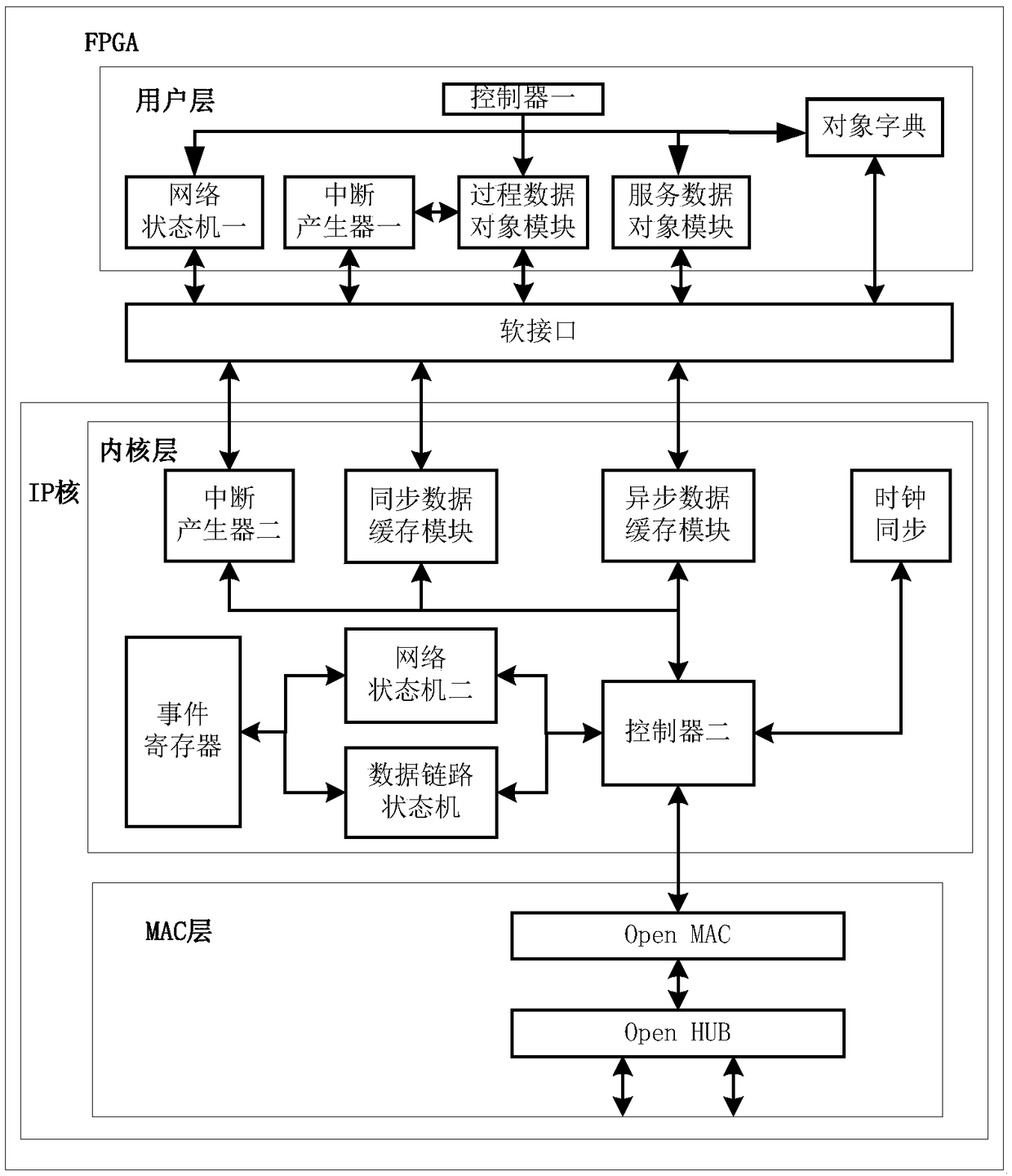
[0097] see image 3 , to adopt figure 2The IP core and the application layer are the same in the Powerlink communication implementation scheme in the same FPGA; the present embodiment realizes a main / power link industrial real-time Ethernet communication in the same FPGA with the IP core of the present invention and the user layer Slave station card design; IP core receives / sends data to user layer through soft interface; IP core receives / sends data to Powerlink network through RJ45 network port;
[0098] The FPGA is responsible for running the entire Powerlink protocol stack, that is, the Powerlink user layer and the kernel layer. In this case, the FPGA chip needs to have integrated microprocessing (such as ARM hard core, or Microblaze soft core, etc.), and the chip also needs to be configured for the CPU. Memory resources (DDR3). Taking Xilinx FPGA as an example, the on-chip soft-core CPU Microblaze is responsible for running the Powerlink user layer code and controlling ...
Embodiment 3
[0134] see Figure 6 , to adopt figure 2 In the middle, the IP core and the application layer are respectively implemented in the Powerlink communication in the FPGA and the microprocessor (microcontroller), and the IP core communicates with the application layer through the CAL interface of the PCIe specification.
[0135] Present embodiment realizes the master / slave station card design of a Powerlink industrial real-time Ethernet communication in FPGA and microprocessor respectively with IP core and user layer described in the present invention, IP core is positioned at FPGA, user layer Located in the bit processor; the IP core receives / sends data to the user layer through the soft interface of the PCIe specification; the IP core receives / sends data to the Powerlink network through the RJ45 network port.
[0136] further, Figure 7 for adoption Figure 6 The block diagram of the internal functional modules of Powerlink communication realized by the scheme. The FPGA in t...
PUM
 Abstract
Description
Claims
Application Information


