Smart skin-oriented optimal design method for chip and wire layouts

A technology of intelligent skinning and design methods, applied in design optimization/simulation, calculation, special data processing applications, etc., can solve problems such as poor practicability, and achieve the effects of enhancing structural load-bearing performance, reducing structural weight, and reducing wire length

Inactive Publication Date: 2018-11-13
NORTHWESTERN POLYTECHNICAL UNIV
View PDF5 Cites 2 Cited by
  • Summary
  • Abstract
  • Description
  • Claims
  • Application Information

AI Technical Summary

Problems solved by technology

[0004] In order to overcome the shortcomings of poor practicability of the existing intelligent skin layout design method, the present invention provides a smart skin-oriented chip and wire layout optimization design method

Method used


Image

  • Smart skin-oriented optimal design method for chip and wire layouts
  • Smart skin-oriented optimal design method for chip and wire layouts
  • Smart skin-oriented optimal design method for chip and wire layouts

Examples


Embodiment Construction

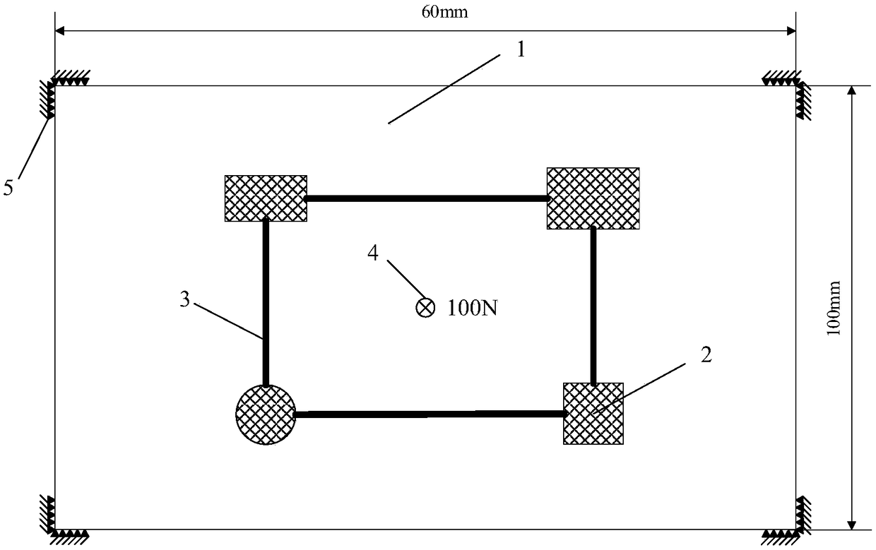
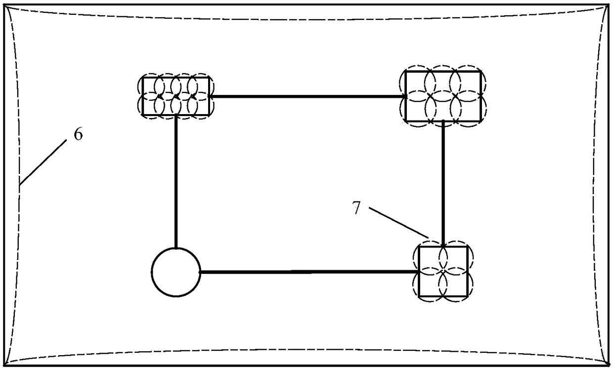
[0026] refer to Figure 1-4 . The specific steps of the intelligent skin-oriented chip and wire layout optimization design method of the present invention are as follows:

[0027] Step 1. Design the detailed structure of the smart skin.

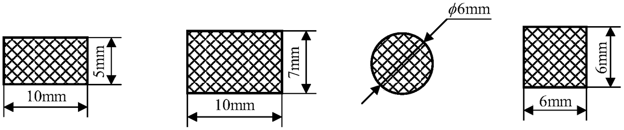
[0028] Taking the three-layer planar intelligent skin circuit board as an example, the three-layer intelligent skin circuit board is 0.2mm, 0.5mm, and 0.2mm thick from top to bottom, and the dimensions of the three layers are all 100mm in length and 50mm in width. The modulus is 4Gpa, the Poisson's ratio is 0.35, and the density is 1450Kg / m 3 ; The Young's modulus of the wire is 75Gpa, the Poisson's ratio is 0.34, and the density is 8900 / m 3 ; The Young's modulus of the filling layer is 0.69Gpa, the Poisson's ratio is 0.4, and the density is 980Kg / m 3 ; The four corners of the matrix structure are fixed, and an out-of-plane force of 100N is applied to the center. There are 4 chips in the middle layer, and the upper limit of the volume of ...


PUM


Abstract

The invention discloses a smart skin-oriented optimal design method for chip and wire layouts, which is used for solving the technical problem that a conventional smart skin layout design method is poor in practicality. According to the technical scheme, a smart skin structure is simulated by using a composite multilayer shell model; the shape of chips is described by using a level set function; and wires among the chips are arranged by using an A* algorithm. In the process of optimizing the layouts, the chips and the wires serve as secondary bearing components to participate in the whole structural force bearing, so that the structural bearing performance is enhanced; in the meantime, the shortest distance among the chip connecting points is found through optimal iteration, so that the wire length and the structure weight are reduced; and proved by tests, under the same conditions, the flexibility of the structure optimized by the method disclosed by the invention was reduced from 91.17mJ of background technology to 9.70mJ and the weight of the structure is reduced from 9.989g of the background technology to 6.315g.

Description

technical field [0001] The invention relates to an intelligent skin layout design method, in particular to an intelligent skin-oriented chip and wire layout optimization design method. Background technique [0002] Smart skins based on sensor networks and various microsystems have broad application prospects. For example, the intelligent skin based on the piezoelectric sensor can not only control the deformation of the wing, but also convert the vibration and other loaded state of the wing into its own electric energy for its use; the stress and strain sensor can monitor the health of the wing in real time. Early warning of skin problems before they occur. Integrating the radar antenna into the skin can greatly reduce the aerodynamic resistance of the aircraft and improve the stealth. [0003] The document "Chinese Invention Patent with Patent Application No. 201510345220.2" discloses a strain sensor layout method for smart skin antennas. This method takes the position and...

Claims


Application Information

Patent Timeline
Patent Type & Authority Applications(China)
IPC IPC(8): G06F17/50
CPCG06F30/23G06F30/392
Inventor 陈飞张卫红朱继宏杜鑫鑫谷小军
Owner NORTHWESTERN POLYTECHNICAL UNIV
Why Eureka
Try Eureka