Pixel structure, driving method thereof and display device

A technology of pixel structure and drive transistor, which is applied in the direction of static indicators, instruments, semiconductor devices, etc., can solve the problems of AMOLED display display quality degradation, inconsistent brightness, and drive current difference, so as to improve the uniformity and stability of display brightness, The effect of eliminating hysteresis and improving response speed

Inactive Publication Date: 2018-11-13
KUNSHAN GO VISIONOX OPTO ELECTRONICS CO LTD
View PDF6 Cites 8 Cited by
  • Summary
  • Abstract
  • Description
  • Claims
  • Application Information

AI Technical Summary

Problems solved by technology

Current AMOLED display panels generally use low-temperature polysilicon (LTPS) substrates. When fabricating TFT arrays on LTPS substrates, the threshold voltage (Vth ) is uneven, so that the driving current generated by each TFT is also different, which in turn causes the brightness emitted by each OELD to be inconsistent, which affects the display effect of the AMOLED display; in addition, when the size of the AMOLED display panel becomes larger, the TFT The problem of IR voltage drop on the power supply (VDD) trace of the power supply of the array will also become more serious, which will cause the received VDD on each TFT to be different, and then cause the drive current generated by each TFT to be different in operation. This will further cause the display quality of the AMOLED display to decline.

Method used


Image

  • Pixel structure, driving method thereof and display device
  • Pixel structure, driving method thereof and display device

Examples


Embodiment Construction

[0031] In order to make the purpose and features of the present invention more obvious and understandable, the specific implementation of the present invention will be further described below in conjunction with the accompanying drawings. However, the present invention can be implemented in different forms and should not be limited to the described embodiments. In addition, the drawings are for illustration purposes only and are not drawn to original scale. For ease of understanding, the same components will be described with the same symbols in the following description. The terms "first", "second", etc. used herein are not intended to refer to the order or sequence, nor are they used to limit the present invention. They are only used to distinguish elements or components described with the same technical terms. Operation only.

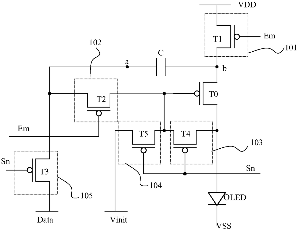
[0032] figure 1 It is a schematic diagram of a pixel structure according to an embodiment of the present invention. Please refer to figure 1 An ...


PUM


Abstract

The invention provides a pixel structure, a driving method thereof and a display device. The pixel structure comprises an LED (light emitting diode), a drive transistor, a memory capacitor, a data receiving unit, a first switch unit, a second switch unit, a first compensation unit and a second compensation; or the pixel structure comprises an LED, a drive transistor, a memory capacitor, a first switching transistor, a second switching transistor, a third switching transistor, a fourth switching transistor and a fifth switching transistor. According to the scheme, the hysteresis effect of the drive transistor can be eliminated, the response speed is increased, uneven brightness caused by threshold voltage shift of the drive transistor can be avoided, and IR pressure drop of a power line canbe compensated, so that display brightness evenness and stability of the display device are improved greatly.

Description

technical field [0001] The present invention relates to the field of display technology, in particular to a pixel structure, a driving method thereof, and a display device. Background technique [0002] Organic light-emitting diodes (OLEDs), as a current-mode light-emitting device, have been increasingly used in high-performance displays. In terms of Active Matrix OLED (AMOLED), the pixel area usually includes an organic light emitting diode (OLED) and a thin film transistor (TFT), and the OLED is generated by the TFT and the current generated during its operation. drive. Current AMOLED display panels generally use low-temperature polysilicon (LTPS) substrates. When fabricating TFT arrays on LTPS substrates, the threshold voltage (Vth ) is uneven, so that the driving current generated by each TFT is also different, which in turn causes the brightness emitted by each OELD to be inconsistent, which affects the display effect of the AMOLED display; in addition, when the size ...

Claims


Application Information

Patent Timeline
Patent Type & Authority Applications(China)
IPC IPC(8): G09G3/3225H01L27/32
CPCG09G3/3225G09G2320/0233H10K59/123H10K59/1213H10K59/1216
Inventor 朱雪婧黄秀颀朱晖张九占孙光远
Owner KUNSHAN GO VISIONOX OPTO ELECTRONICS CO LTD
Why Eureka
Try Eureka