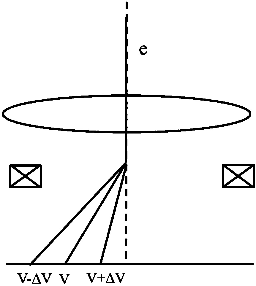
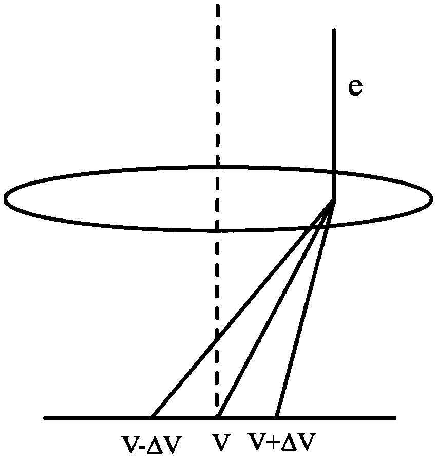
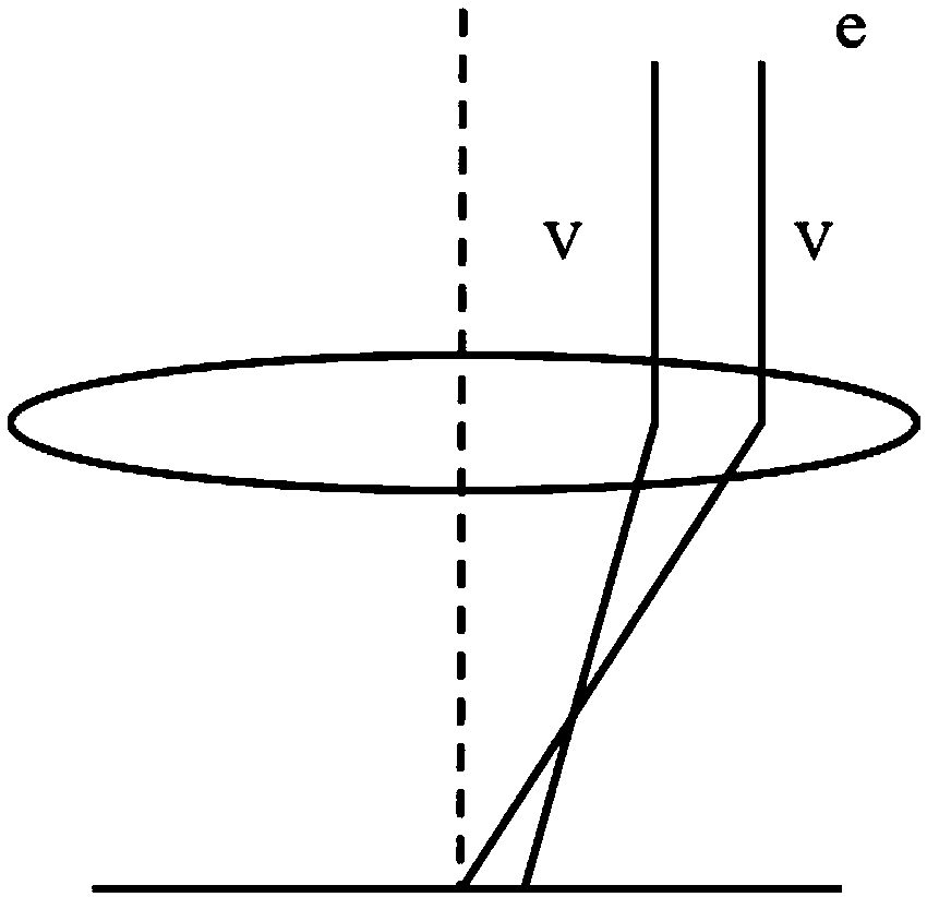
Scanning electron microscope system and sample detection method
A technology for electron microscopes and samples, applied in circuits, discharge tubes, electrical components, etc., to solve problems such as decreased resolution and increased focused beam spot
- Summary
- Abstract
- Description
- Claims
- Application Information
AI Technical Summary
Problems solved by technology
Method used
Image
Examples
Embodiment 1
[0046] An optional schematic diagram of a scanning electron microscope system provided in Embodiment 1 of the present invention, such as Figure 4 As shown, it includes: an electromagnetic cross-field analyzer 105 , a composite objective lens 11 composed of an electric lens 10 and a magnetic lens 107 , a rear deflection device 108 and a sample stage 109 .
[0047] In some embodiments, the function of the electromagnetic cross-field analyzer 105 can be implemented by a Wien analyzer. The electromagnetic cross-field analyzer 105 is located between the upper pole piece of the magnetic lens 107 and the electron source 101 that generates the initial electron beam incident to the scanning electron microscope, and the central area of the electromagnetic cross-field analyzer 105 coincident with the optical axis.
[0048] Here, the initial electron beam incident to the scanning electron microscope system is generated and emitted by the electron source 101, and the electrons emitted ...
Embodiment 2
[0062] The scanning electron microscope system provided by the second embodiment of the present invention is similar to the scanning electron microscope system provided by the first embodiment of the present invention, the difference is that the composition structure of the scanning electron microscope system provided by the second embodiment of the present invention is as follows Figure 9 As shown, a high-voltage tube 202 is also included; the high-voltage tube 202 is located between the upper pole piece of the magnetic lens 107 and the electron source that generates the initial electron beam incident to the scanning electron microscope system, and the center of the high-voltage tube 202 axis coincides with the optical axis. A higher voltage is loaded on the high-voltage tube 202, and the initial electron beam sent by the electron source 101 will maintain higher energy through the high-voltage tube 202, thereby reducing the influence of the space charge effect; the electric l...
Embodiment 3
[0064] Based on the scanning electron microscope system described in Embodiment 1 and Embodiment 2 above, Embodiment 3 of the present invention also provides a sample detection method. An optional processing flow of the sample detection method is as follows: Figure 10 shown, including the following steps:
[0065] In step S101, the initial electron beam emitted by the electron source is focused and incident on the surface of the sample to be tested under the action of the composite objective lens.
[0066] In the embodiment of the present invention, before the initial electron beam is incident on the composite objective lens of the scanning electron microscope, the electromagnetic cross-field analyzer and the deflection device behind the mirror are turned off first, and turning off the electromagnetic cross-field analyzer means that no voltage is applied to the electromagnetic cross-field analyzer and current, turning off the deflection device behind the mirror means not load...
PUM
 Abstract
Description
Claims
Application Information
 - R&D
- Intellectual Property
- Life Sciences
- Materials
- Tech Scout
- Unparalleled Data Quality
- Higher Quality Content
- 60% Fewer Hallucinations
Browse by: Latest US Patents, China's latest patents, Technical Efficacy Thesaurus, Application Domain, Technology Topic, Popular Technical Reports.
© 2025 PatSnap. All rights reserved.Legal|Privacy policy|Modern Slavery Act Transparency Statement|Sitemap|About US| Contact US: help@patsnap.com


