Assembled circuit board detection system and assembled circuit board detection method

A technology for assembling circuit boards and inspection systems, applied in electrical components, electrical components, optical testing flaws/defects, etc., can solve problems such as inefficiency, inability to maintain assembled circuit boards, and increased rework costs.

Active Publication Date: 2018-11-13
GIGA BYTE TECH CO LTD
View PDF11 Cites 3 Cited by
  • Summary
  • Abstract
  • Description
  • Claims
  • Application Information

AI Technical Summary

Problems solved by technology

However, due to the current situation that the hardware equipment of the test machine is individually set independently, the test items that can theoretically be processed at the same time must be divided into multiple stations to carry out sequentially, resulting in an extremely long total test time for a single assembled circuit board and inefficient
In addition, due to the large number of DIP parts on the assembled circuit board, the operator who cooperates with the test machine is prone to make mistakes in the visual inspection process due to factors such as negligence and fatigue, resulting in the failure of the assembled circuit board to maintain a stable yield rate, and therefore additional Increase the cost of rework after the test goes wrong

Method used


Image

  • Assembled circuit board detection system and assembled circuit board detection method
  • Assembled circuit board detection system and assembled circuit board detection method
  • Assembled circuit board detection system and assembled circuit board detection method

Examples


Embodiment Construction

[0039] The detailed features and advantages of the present invention are described in detail below in the embodiments, the content of which is sufficient to enable any person familiar with the relevant art to understand the technical content of the present invention and implement it accordingly, and according to the content disclosed in this specification, the patent scope of the application and the drawings , anyone skilled in the relevant art can easily understand the related objects and advantages of the present invention. The following examples are to further describe the present invention in detail, but not to limit the scope of the present invention in any way.

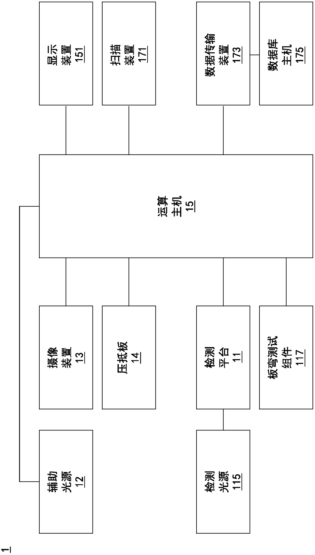
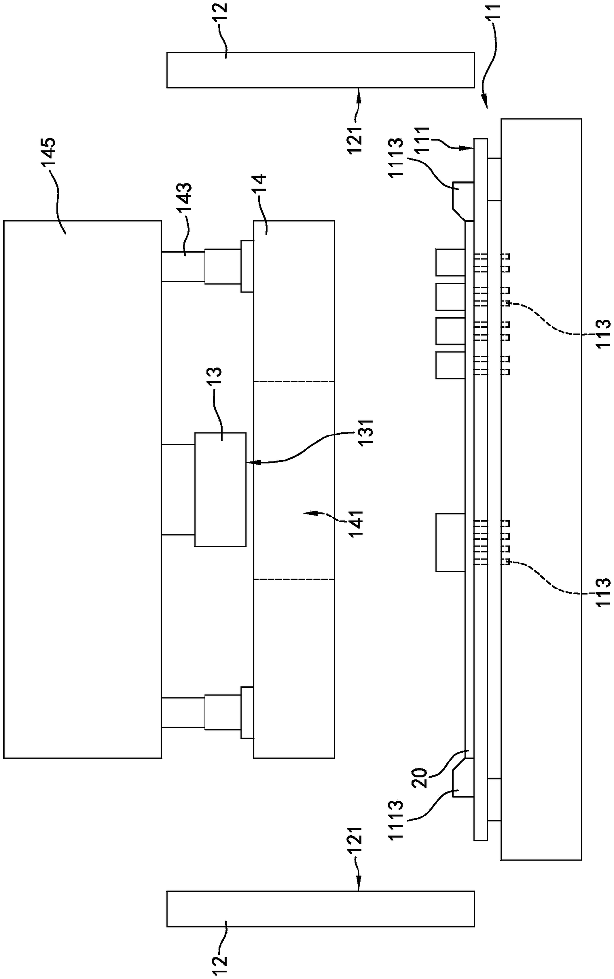
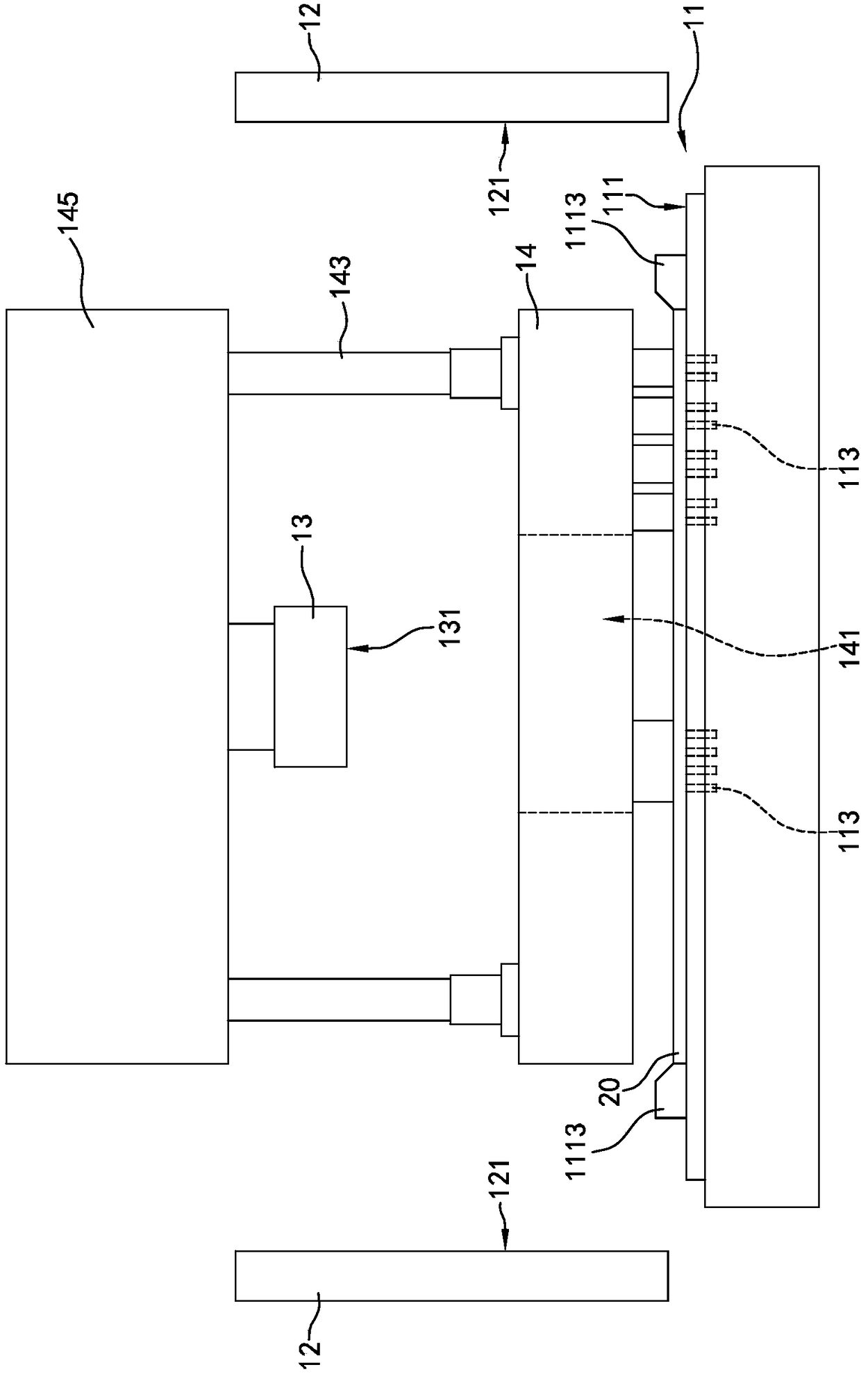
[0040] The assembly circuit board inspection system and assembly circuit board inspection method of the present invention are suitable for an assembly circuit board with soldered DIP parts. Please also refer to figure 1 and Figure 2A , figure 1 It is a functional block diagram of an assembly circuit board in...


PUM


Abstract

The invention relates to an assembled circuit board detection system. The system includes a detection platform, an image pickup device, a pressing and abutting plate and a computing host; the detection platform is provided with a carrying surface which is used for carrying an assembled circuit board and is provided with a plurality of circuit detection contacts; the image pickup device photographsthe assembled circuit board on the carrying surface to generate an image to be detected; the pressing and abutting plate is movably disposed between the detection platform and the image pickup device; the pressing and abutting plate is provided with a light transmitting portion aligned with the image pickup device; the pressing and abutting plate is used for pressing and abutting against the assembled circuit board, so that the connection pins of the plurality of material components of the assembled circuit board can be electrically connected with the circuit detection contacts; the computinghost is electrically connected with the detection platform and the image pickup device so as to receive the image to be detected, execute an image analysis program and test the material components ofthe assembled circuit board through the detection platform.

Description

technical field [0001] The present invention relates to an assembled circuit board inspection system and an assembled circuit board inspection method, in particular to an assembled circuit board inspection system integrating Automated-Optical Inspection (AOI) and In Circuit Tester (ICT) And the detection method of assembled circuit board. Background technique [0002] In the process of manufacturing electronic products, various electronic components must be assembled on a printed circuit board (PCB). These electronic components can usually adopt surface mount technology (Surface Mount Technology, SMT) or dual in-line package (Dual In Line Package, DIP) process. Among them, the assembly method of DIP process parts is to insert the pins of DIP parts into the plating through hole (PTH) on the printed circuit board, and apply flux on the bottom of the printed circuit board, and then solder the parts through the solder furnace. It is fixed on the printed circuit board, and then...

Claims


Application Information

Patent Timeline
Patent Type & Authority Applications(China)
IPC IPC(8): H05K13/08G01N21/95
CPCG01N21/95H05K13/08
Inventor 吕纪纬孟宪明孙武雄陈烱奇廖祝湘张基霖王瑞志郑宗宪
Owner GIGA BYTE TECH CO LTD
Why Eureka
Try Eureka