Pixel circuit and driving method thereof, display panel and display device

A pixel circuit and electrode technology, applied in the field of flat-panel display, can solve the problems of brightness change of organic light-emitting elements, uneven threshold voltage of driving transistors, affecting image display effect, etc., so as to avoid the reduction of gate voltage and solve the problem of uneven display brightness. , improve the display effect

Active Publication Date: 2018-11-20
KUNSHAN GO VISIONOX OPTO ELECTRONICS CO LTD
View PDF8 Cites 22 Cited by
  • Summary
  • Abstract
  • Description
  • Claims
  • Application Information

AI Technical Summary

Problems solved by technology

Due to the process and device aging, there will be non-uniformity in the threshold voltage of the driving transistor of the pixel circuit, which will cause the current flowing through different OLED pixels to change, resulting in uneven display brightness, thereby affecting the display effect of the entire image.
[0004] At present, this problem is mainly solved through the internal compensation function of the pixel circuit. Generally, the internal compensation of the pixel circuit can be realized only through the pixel circuit with compensation function. The pixel circuit is generally a 7T1C (7 transistors and 1 capacitor) circuit. However, in the data writing stage of the 7T1C circuit, due to the characteristics of the transistor itself, a small current will still flow when it is turned off, which reduces the gate voltage of the driving transistor, making the brightness of the organic light-emitting element change with time, forming a flickering problem

Method used


Image

  • Pixel circuit and driving method thereof, display panel and display device
  • Pixel circuit and driving method thereof, display panel and display device
  • Pixel circuit and driving method thereof, display panel and display device

Examples


Embodiment Construction

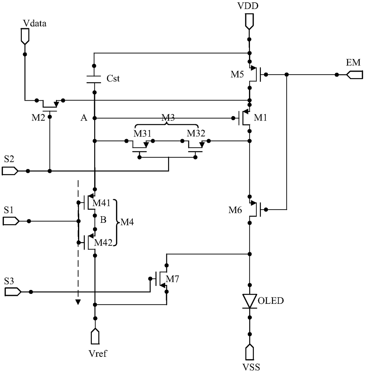
[0034] figure 1 is a schematic diagram of the structure of a pixel circuit, such as figure 1 As shown, the pixel circuit includes: a first transistor M1, a second transistor M2, a third transistor M3, a fourth transistor M4, a fifth transistor M5, a sixth transistor M6, a seventh transistor M7, a storage capacitor Cst, and an organic light-emitting Element OLED.

[0035] The gate of the first transistor M1 is connected to the first end of the storage capacitor Cst, the first electrode of the first transistor M1 is connected to the first electrode of the second transistor M2, and the first transistor M1 The second electrode of is connected to the first electrode of the third transistor M3. The gate of the second transistor M2 is connected to the second scan signal terminal S2, and the second electrode of the second transistor M2 is connected to the data signal terminal Vdata. The gate of the third transistor M3 is connected to the second scan signal terminal S2, and the seco...


PUM


Abstract

The invention provides a pixel circuit and a driving method thereof, a display panel and a display device. The pixel circuit comprises eight transistors, two storage capacitors and an organic light emitting device (OLED), a threshold voltage of the first transistor is compensated through mutual cooperation of the transistors and the capacitors, a driving current for driving the OLED to emit lightis made to be independent of the threshold voltage of the first transistor, so influence of fluctuation of the threshold voltage of the first transistor on the OLED is avoided, a problem of uneven display brightness caused by this is solved, the display effect of the whole frame is improved, moreover, since the leakage current between the first storage capacitor and the second storage capacitor can be reduced by the eighth transistor, reduction of a gate voltage of the first transistor is avoided, a problem of scintillation caused by the leakage current is solved, and the display effect of thewhole display frame is further improved.

Description

technical field [0001] The present invention relates to the technical field of flat panel display, in particular to a pixel circuit and a driving method thereof, a display panel and a display device. Background technique [0002] Organic Light Emitting Diode (OLED) is one of the hot spots in the field of display research today. Compared with Liquid Crystal Display (LCD), OLED has the advantages of low energy consumption, low production cost, self-luminescence, wide viewing angle and The advantages of fast response and so on. At present, OLED displays have begun to replace traditional LCD displays in display fields such as mobile phones, PDAs, and digital cameras. Among them, pixel circuit design is the core technical content of OLED displays, which has important research significance. [0003] Unlike LCD, which uses a stable voltage to control brightness, OLED is current-driven and requires a stable current to control light emission. Due to reasons such as process and dev...

Claims


Application Information

Patent Timeline
Patent Type & Authority Applications(China)
IPC IPC(8): G09G3/3266G09G3/3233
CPCG09G3/3233G09G3/3266G09G2320/0233
Inventor 段培金波
Owner KUNSHAN GO VISIONOX OPTO ELECTRONICS CO LTD
Why Eureka
Try Eureka