Electronic device with low stress and high overload resistance and packaging method of electronic device

An electronic device and packaging method technology, applied in the packaging field of electronic devices, can solve the problems of large contact area, low stress on electronic chips, and no coverage by any objects, and achieves the effect of low packaging stress

Pending Publication Date: 2018-11-23
ANHUI BEIFANG XINDONG LIANKE MICROSYST TECH
View PDF3 Cites 4 Cited by
  • Summary
  • Abstract
  • Description
  • Claims
  • Application Information

AI Technical Summary

Problems solved by technology

However, in this method, the contact area between the electronic chip and the soft glue is large, and the thermal expansion coefficients of the soft glue and the electronic chip differ greatly, so the stress generated by the soft glue will also affect the performance of the electronic chip that is very sensitive to stress; moreover, The surface of the electronic chip is fully or partially covered with soft glue, and some types of electronic chips, such as

Method used


Image

  • Electronic device with low stress and high overload resistance and packaging method of electronic device
  • Electronic device with low stress and high overload resistance and packaging method of electronic device
  • Electronic device with low stress and high overload resistance and packaging method of electronic device

Examples


Embodiment 1

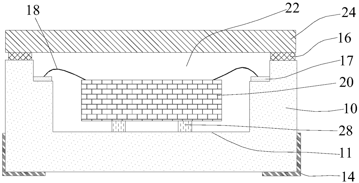
[0040] Electronics with low stress and high overload resistance at the same time, such as Figure 10 As shown, it includes a package shell 10, a package cover plate 24 and an electronic chip 20. The package cover plate 24 is combined with the package tube shell 10 by solder 16 to form a sealed cavity 22 for protecting the electronic chip 20. The package cover plate 24 The material can be plastic, ceramics, Kovar, glass, germanium, silicon, etc., and the material of the package package 10 can be plastic, ceramics, etc. On the inner surface 24a of the package cover plate 24, a patterned upper protective soft rubber 33 is made. The soft glue 33 can buffer mechanical force, protect the electronic chip 20 from colliding with the packaging cover plate 24, and because the upper protective soft glue 33 is very soft, even if the electronic chip 20 collides with it, it will not cause damage. The figure of the upper protective soft glue 33 is Square, rectangular, circular, etc., there i...

Embodiment 2

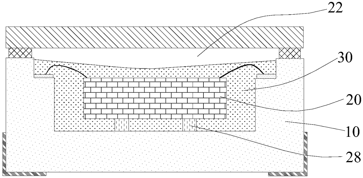
[0050] Electronics with low stress and high overload resistance at the same time, such as Figure 11 As shown, it includes a package shell 10, a package cover plate 24 and an electronic chip 20. The package cover plate 24 is combined with the package tube shell 10 by solder 16 to form a sealed cavity 22 for protecting the electronic chip 20. The package cover plate 24 The material can be plastic, ceramics, Kovar, glass, germanium, silicon, etc., and the material of the package package 10 can be plastic, ceramics, etc. On the inner surface 24a of the package cover 24, a patterned upper protective soft rubber 33 is made. The hardness of the material is relatively low, such as silicone or epoxy glue with a Shore hardness of 20-100. The soft glue 33 can buffer mechanical force, protect the electronic chip 20 from colliding with the packaging cover plate 24, and because the upper protective soft glue 33 is very soft, even if the electronic chip 20 collides with it, it will not caus...

Embodiment 3

[0053] Electronics with low stress and high overload resistance at the same time, such as Figure 12As shown, it includes a package shell 10, a package cover plate 24 and an electronic chip 20. The package cover plate 24 is combined with the package tube shell 10 by solder 16 to form a sealed cavity 22 for protecting the electronic chip 20. The package cover plate 24 The material can be plastic, ceramics, Kovar, glass, germanium, silicon, etc., and the material of the package package 10 can be plastic, ceramics, etc. On the inner surface 24a of the package cover 24, a patterned upper protective soft rubber 33 is made. The hardness of the material is relatively low, such as silicone or epoxy glue with a Shore hardness of 20-100. The soft glue 33 can buffer mechanical force, protect the electronic chip 20 from colliding with the packaging cover plate 24, and because the upper protective soft glue 33 is very soft, even if the electronic chip 20 collides with it, it will not cause...


PUM

PropertyMeasurementUnit
Diameteraaaaaaaaaa
Heightaaaaaaaaaa

Abstract

The invention discloses an electronic device with low stress and high overload resistance and a packaging method of the electronic device. Protection flexible glue is dropwise added on the inner sideof a bottom plate of a packaging tube shell, and pressing is performed to form lower protection flexible glue and side protection flexible glue; the protection flexible glue is dropwise added on the inner surface of a packaging cover plate, and pressing is performed to form patterned upper protection flexible glue; then a bonding piece glue point is dropwise added to the lower protection flexibleglue to enable an electronic chip to be attached to the packaging tube shell, and it is ensured that there is no direct mechanical connection between the electronic chip and the inner side surface ofthe packaging tube shell and between the electronic chip and the packaging cover plate; then metal wires are bonded, and finally, covering of the packaging cover plate is performed. By virtue of the upper protection flexible glue, the lower protection flexible glue and the bonding piece glue point, external force impact in the Z direction can be buffered jointly, so that the electronic chip is protected from collision with the packaging cover plate or the bottom plate of the packaging tube shell; and by virtue of the side protection flexible glue, external force impact in the X-axis directionand the Y-axis direction can be buffered, so that the electronic chip is protected from collision with the side surface of the packaging tube shell, thereby enabling the electronic device to resist high overload and to be relatively low in packaging stress.

Description

technical field [0001] The invention relates to packaging of electronic devices, in particular to an electronic device with low stress and high overload resistance and a packaging method thereof. Background technique [0002] Electronic device packaging is to electrically connect one or more electronic device chips to each other, and then encapsulate them in a protective structure to provide electrical connection, mechanical protection, chemical corrosion protection, etc. for the electronic chips. For some sensor products in industrial applications, due to the consideration of performance and reliability, especially the consideration of reducing the impact of stress, the cavity packaging method is often used, that is, the electronic chip is mounted on the bottom plate of the preformed package through adhesive , bonding the metal wires to lead the electrical signal of the chip out of the package shell, and finally sealing the package shell with a cover plate. Some electronic...

Claims


Application Information

Patent Timeline
IPC IPC(8): H01L23/24H01L21/50
CPCH01L21/50H01L23/24H01L2224/48227H01L2224/48091H01L2224/83385H01L2924/16195H01L2924/15153H01L2924/00014
Inventor 华亚平
Owner ANHUI BEIFANG XINDONG LIANKE MICROSYST TECH
Why Eureka
Try Eureka