
Electronic component and printed circuit board

A technology of electronic components and components, applied in the directions of printed circuits, printed circuits, printed circuit manufacturing, etc., can solve the problems of poor measurement accuracy, release, etc.

Active Publication Date: 2018-11-23
SCHWEIZER ELECTRONIC
View PDF10 Cites 0 Cited by
  • Summary
  • Abstract
  • Description
  • Claims
  • Application Information

AI Technical Summary

Problems solved by technology

[0005] Surface-mounted components have the disadvantage that the generated power losses are released to the environment by convection
The measurement accuracy when using this type of shunt is degraded due to the change in material resistance caused by the increase in temperature

Method used


Image

  • Electronic component and printed circuit board
  • Electronic component and printed circuit board
  • Electronic component and printed circuit board

Examples


Embodiment Construction

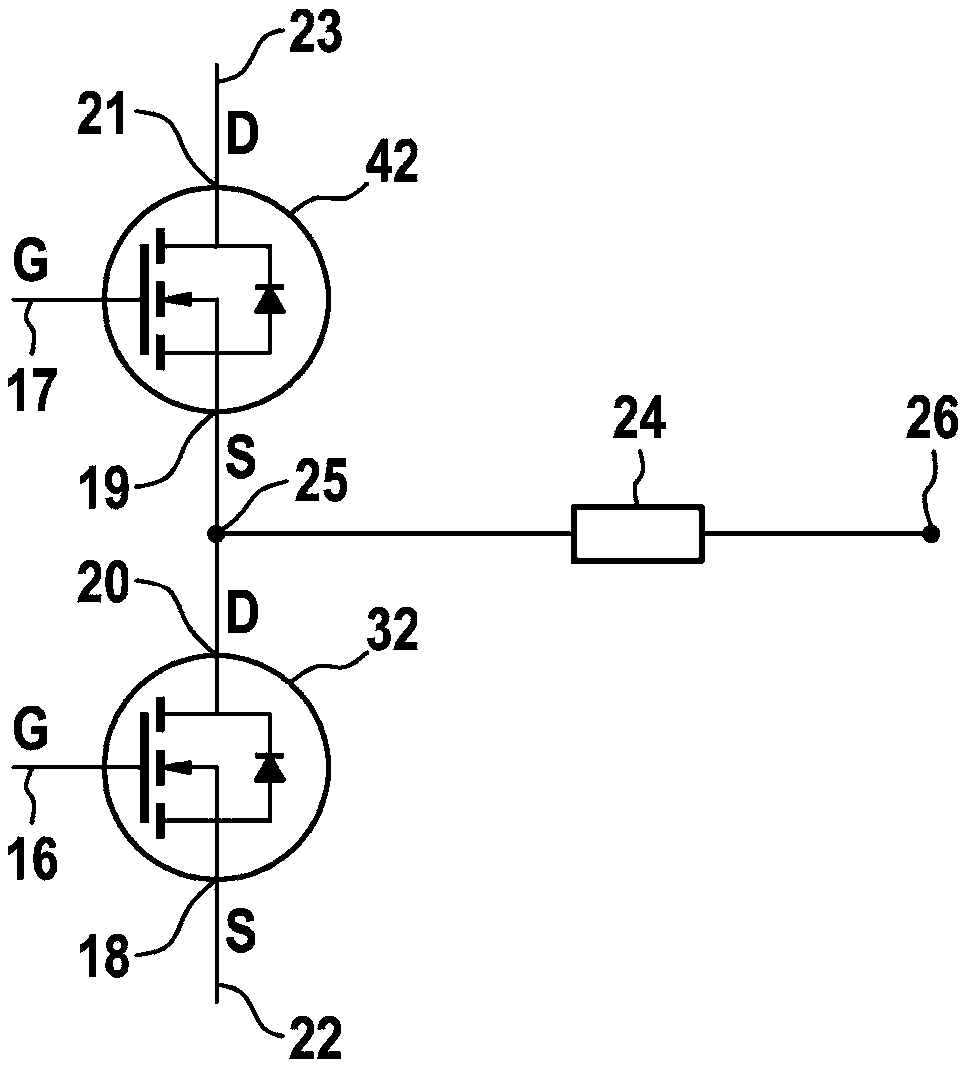
[0051] The electronic component in the half-bridge form according to the present invention includes a first semiconductor component 32 and a second semiconductor component 42. The semiconductor components 32, 42 have gate terminals 16, 17, source terminals 18, 19, and drain terminals 20, 21, respectively. The external contact 23 of the second semiconductor component 42 is connected to the positive electrode of a voltage source not shown. The external contact 22 of the first semiconductor component 32 is connected to the negative electrode of the voltage source. The shunt element 24 is arranged between the midpoint 25 of the half bridge and the phase tap 26.

[0052] The gate terminals 16, 17 of the two semiconductor devices 32, 42 are activated alternately, so that the semiconductor components 32, 42 alternately allow current to flow between their drain terminals 20, 21 and their source terminals 18, 19 Over. The AC voltage can be generated in this way at the midpoint 25 of th...


PUM


Abstract

The invention relates to an electronic component and a printed circuit board. The electronic component has a first lead frame (31) consisting of an electrically conductive material. The first lead frame (31) carries a first semiconductor component (32). In the plane of the lead frame (31), a shunt element (34) is arranged, wherein the shunt element (34) comprises a resistor body (37) arranged between a first terminal contact (35) and a second terminal contact (36). An electrically conducting connection member (44) extends from a terminal (20) of the first semiconductor component (32) through the first lead frame (31) to the first terminal contact (35) of the shunt element (34). A current measurement with good accuracy is facilitated.

Description

Technical field [0001] The present invention relates to an electronic component having a first lead frame made of conductive material. The first lead frame carries the first semiconductor component. Background technique [0002] It is known that conductive lead frames are used in electronic components to draw current from semiconductor components, EP 2524 394 A2. In particular, a larger current intensity can be transmitted via this lead frame, which is advantageous for use in power electronic devices. [0003] If the aim is to measure the intensity of the current flowing through the semiconductor component, then the current can pass through a low value resistor (shunt) and measure the voltage drop across the resistor, DE 10 2016 003 988A1. From the pressure drop, it is possible to deduce the current intensity and then the energy consumption. [0004] In order to minimize the consumption or loss of power during the current measurement, a shunt with an extremely small resistance, fo...

Claims


Application Information

Patent Timeline
Patent Type & Authority Applications(China)
IPC IPC(8): H01L23/495H05K1/09
CPCH01L23/495H05K1/09H01L23/492H01L23/62H01L2224/18G01R1/203H05K1/185H05K2201/10166H05K3/4602H01L23/49575H01L23/5329H01L23/53228H01L23/49568H01L23/49582H01L23/49586H05K1/181
Inventor 托马斯·戈特瓦尔德克里斯蒂安·勒斯勒
Owner SCHWEIZER ELECTRONIC
Learn More