Display device and fabrication method thereof

A display device and drain layer technology, which is applied in semiconductor/solid-state device manufacturing, electrical components, transistors, etc., can solve problems such as load effect, reliability reduction, and poor film coverage, so as to improve reliability and avoid Load effect, effect of improving coverage

Inactive Publication Date: 2018-11-23
WUHAN CHINA STAR OPTOELECTRONICS TECH CO LTD
View PDF4 Cites 1 Cited by
  • Summary
  • Abstract
  • Description
  • Claims
  • Application Information

AI Technical Summary

Problems solved by technology

[0003] In the current technology, the sides of the source / drain will be etched when preparing the subsequent film layer, resulting in poor film coverage, load effect, and reduced reliability

Method used


Image

  • Display device and fabrication method thereof
  • Display device and fabrication method thereof
  • Display device and fabrication method thereof

Examples


Embodiment Construction

[0023] The following will clearly and completely describe the technical solutions in the embodiments of the application with reference to the drawings in the embodiments of the application. Apparently, the described embodiments are only some of the embodiments of the application, not all of them. Based on the embodiments in this application, all other embodiments obtained by persons of ordinary skill in the art without making creative efforts belong to the scope of protection of this application.

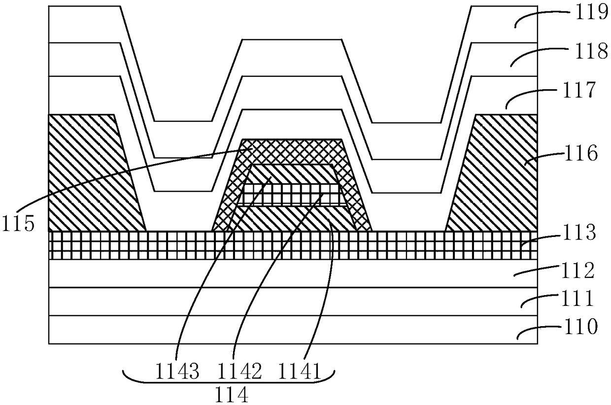
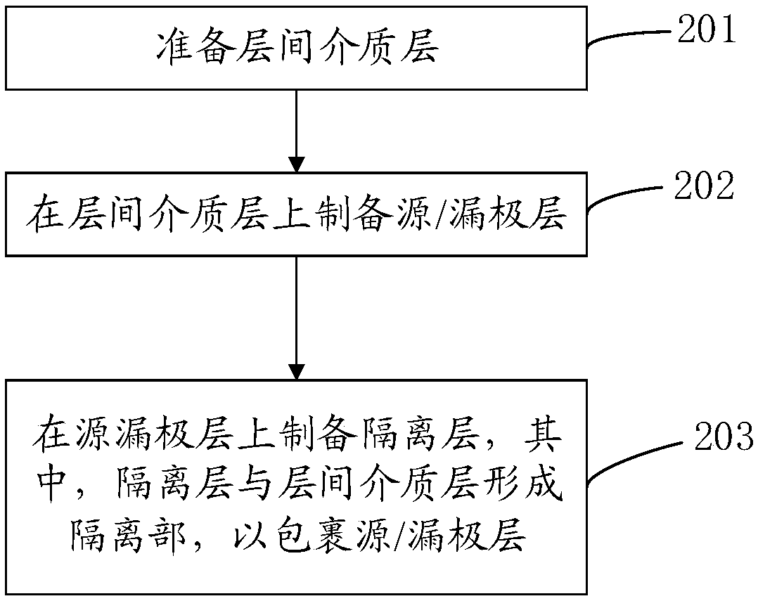
[0024] The present application provides a display device, including an interlayer dielectric layer, a source / drain layer, and an isolation layer arranged in sequence, wherein the isolation layer and the interlayer dielectric layer form an isolation portion to wrap the source / drain layer.

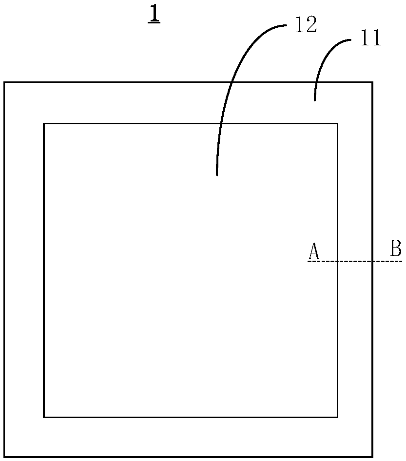
[0025] In order to clearly illustrate the specific structure of the display device of this application, please refer to figure 1 , figure 1 is a schematic plan view of an embodiment of the displa...


PUM


Abstract

The invention discloses a display device and a fabrication method thereof. The display device comprises an interlayer dielectric layer, a source / drain layer and an isolation layer which are sequentially arranged, wherein the isolation layer and the interlayer dielectric layer form an isolation part to wrap the source / drain layer. In the display device, the source / drain layer is wrapped by the isolation layer and the interlayer dielectric layer, so that the source / drain layer is prevented from being corroded by an etching liquid in subsequent processes, the coverage of a film layer can be improved, a load effect is prevented, and the reliability is improved.

Description

technical field [0001] The present application relates to the field of display technology, in particular to a display device and a manufacturing method thereof. Background technique [0002] With the development of the panel industry, the mobile phone screen LTPS (Low Temperature Poly-silicon, low temperature polysilicon technology) process technology gradually replaces a-Si. Its carrier mobility is high, and the driving circuit can be fabricated on the TFT substrate. In addition, because of its higher mobility, the size of TFT is smaller than that of a-Si products, and the screen aperture ratio is higher. With the development of LTPS process, In Cell Touch Panel (embedded touch screen) technology is more used in the industry. Compared with the traditional process, Touch is made on TFT substrate, which is more conducive to the thinning and lightening of mobile phones. The process development for In cell touch panel tends to reduce the number of processes. [0003] In the ...

Claims


Application Information

Patent Timeline
Patent Type & Authority Applications(China)
IPC IPC(8): H01L27/12H01L29/786H01L21/77
CPCH01L27/1248H01L27/1259H01L29/78636
Inventor 张嘉伟
Owner WUHAN CHINA STAR OPTOELECTRONICS TECH CO LTD
Why Eureka
Try Eureka