Optical waveguide laminated body and manufacturing method therefor

A manufacturing method, optical waveguide technology, applied in the direction of optical waveguide light guide, optical waveguide coupling, light guide, etc., to achieve the effect of excellent insulation and heat resistance, excellent processing accuracy, and efficient removal processing

Active Publication Date: 2018-11-23
NITTO DENKO CORP
View PDF28 Cites 0 Cited by
  • Summary
  • Abstract
  • Description
  • Claims
  • Application Information

AI Technical Summary

Problems solved by technology

[0010] In addition, in the case where the photoelectric hybrid board 10 is used as a connector for connection, as in Figure 11 As shown in (a), it is necessary to insert and fix the top portion of the opto-electric hybrid board 10 into the concave portion 11a of the sleeve (Japanese: ferrule) 11, but in order to prevent damage to the protruding portion of the circuit board E However, when the opening of the above-mentioned recessed portion 11a is designed so as to have a large gap with respect to the outer shape of the circuit board E, there arises a problem that the positioning of the core 7 in the recessed portion 11a cannot be performed correctly, and the connection based on the connector cannot be properly performed. optical coupling

Method used


Image

  • Optical waveguide laminated body and manufacturing method therefor
  • Optical waveguide laminated body and manufacturing method therefor
  • Optical waveguide laminated body and manufacturing method therefor

Examples


Embodiment 1~ Embodiment 9、 comparative example 1~ comparative example 4

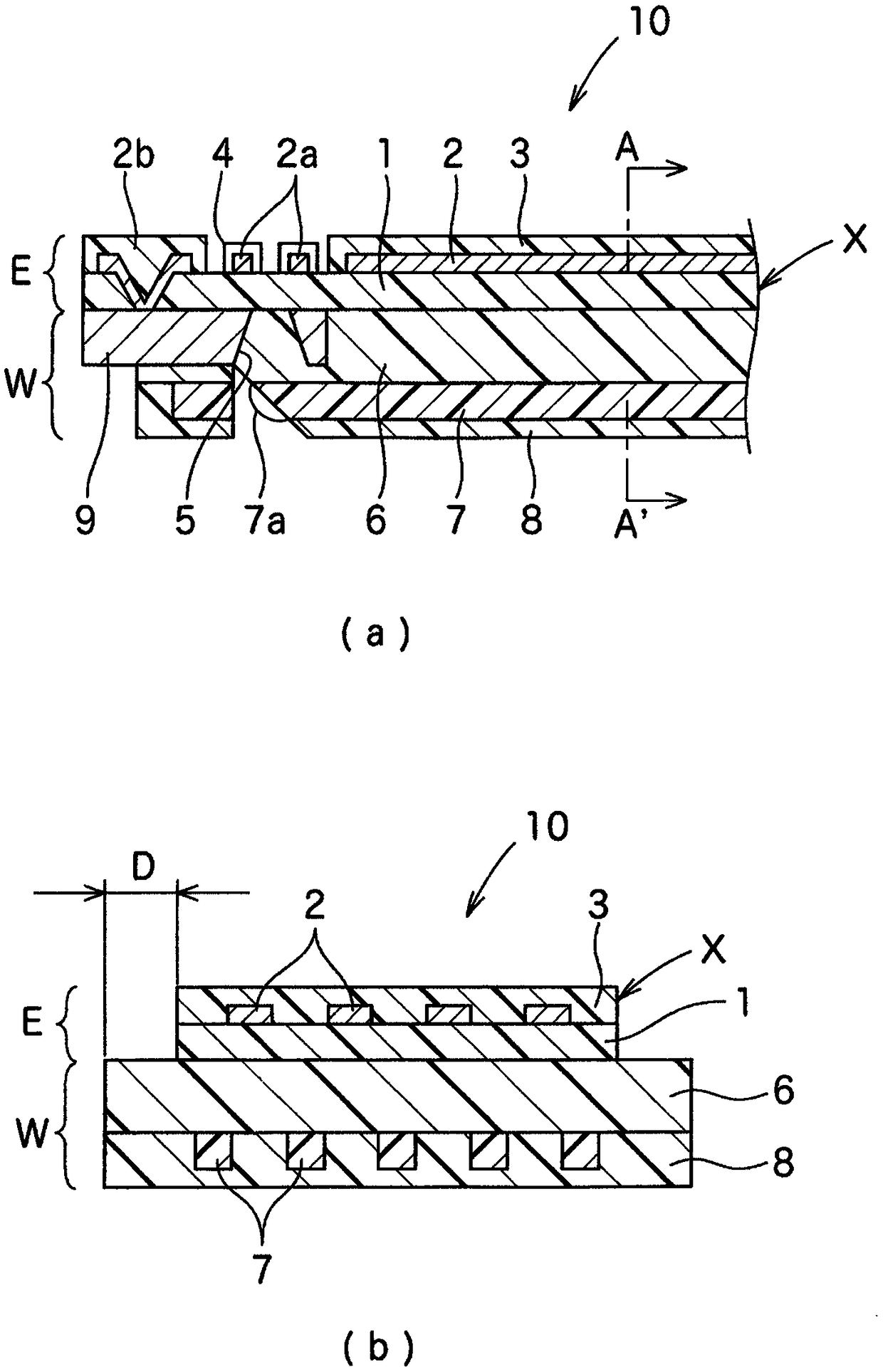
[0086] Using the material used for the optical waveguide W and the material used for the organic substrate layer X described later, the optical waveguide W (overall thickness 110 μm: Clad1 thickness 40 μm + Clad2 thickness 30 μm + Core thickness 40 μm ) by laminating an organic substrate layer X (total thickness 15 μm: thickness of insulating layer 10 μm + thickness of cover layer 5 μm), thereby producing samples simulating 13 kinds of optical circuit boards (Example 1 to Example 9, Comparative Example 1 -Comparative example 4), the combination of the material of the optical waveguide W and the material of the organic base material layer X at the laser processed part of these samples is shown in Table 1 described later. Then, these samples were irradiated with laser light in the thickness direction of the sample using four types of laser devices described later to remove the organic base material layer X only at one edge portion (region with a width of 50 μm) of the sample. Th...


PUM


Abstract

This optical waveguide laminated body has an organic base layer X comprising an insulating layer 1 and a coverlay 3 laminated onto one surface of an optical waveguide W, and has a portion of the organic base layer X removed such that the optical waveguide W is partially exposed through the removed portion. Provided that P represents a transmittance of laser light in a prescribed wavelength range through the optical waveguide W at the exposed optical wave guide part and Q represents a transmittance of the laser light through at least a portion of the organic base layer X facing the exposed optical waveguide part, the P and Q satisfy the following relationships: P >= 70% and P-Q >= 25%. According to the optical waveguide laminated body, the organic base layer laminated onto the optical waveguide is removed with precision without incurring physical and thermal damage due to laser beam machining. As such, the optical waveguide laminated body maintains high quality.

Description

technical field [0001] The present invention relates to an optical waveguide laminate obtained by laminating an organic substrate layer such as an insulating film on at least one surface of an optical waveguide, and a method for producing the same. Background technique [0002] Along with the increase in the amount of information to be transmitted, in recent electronic devices and the like, optical wiring is used in addition to electrical wiring, and an opto-electrical hybrid substrate capable of simultaneously transmitting electrical and optical signals is often used. As such a photoelectric hybrid substrate, for example, the following structures are known: Figure 10 As shown, an insulating layer 1 formed of polyimide or the like is used as a substrate, an electrical wiring 2 formed of a conductive pattern is provided on the surface of the insulating layer 1 to form a circuit substrate E, and a light source is provided on the back side of the insulating layer 1. A waveguid...

Claims


Application Information

Patent Timeline
IPC IPC(8): G02B6/122G02B6/12G02B6/13H05K1/02
CPCG02B1/04G02B1/046G02B1/048G02B6/138G02B6/3885G02B6/4293G02B6/43H05K1/02C08L63/04C08L77/00C08L63/00G02B6/122G02B6/13
Inventor 田中直幸
Owner NITTO DENKO CORP
Why Eureka
Try Eureka