Bidirectional transient voltage suppressor for triggering SCR by diode strings in an auxiliary way

A technology of transient voltage suppression and diode strings, which is applied in the direction of electric solid-state devices, circuits, transistors, etc., can solve problems such as low maintenance voltage and large latch-up risk, and achieve the effect of reducing trigger voltage and enhancing robustness

Active Publication Date: 2018-11-27
JIANGNAN UNIV
5 Cites 8 Cited by

AI-Extracted Technical Summary

Problems solved by technology

However, SCR has the characteristics of high trigger voltage a...

Method used

A kind of bidirectional transient voltage suppressor that the present invention proposes, the equivalent circuit under the effect of reverse electrical stress is as shown in Figure 4, when the first electrical stress terminal of device is grounded, the second electrical stress terminal connects high potential, the diode D3 formed by the second P+ injection region 107 and the N well 103, the diode D4 formed by the P well 104 and the third N+ injection region 110, the diode D3 and the diode D4 pass through the first N+ injection region 106, the metal The line and the third P+ implantation region 109 form a second series path, and when the electrical stress reaches 1.4V, the second series path is turned on. At the same time, the PNP transistor T1 is formed by the first P+ implantation region 105, the N well 103 and the second P+ implantation region 107, and the NPN transistor T2 composed of the second N+ implantation region 108, the P well 104 and the third N+ implantation region 110 is composed of The NPN transistor T5 formed by the N well 103, the P well 104, and the third N+ implantation region 110 and the PNP transistor T6 formed by the second P+ implantation region 107, the N well 103 and the P well 104 all start to work in an amplified state, which can improve the performance of the device. current discharge capability. The second SCR structure composed of the PNP transistor T5 and the NPN transistor T6 is beneficial to further enhance the robustness of the de...

Abstract

The invention relates to a bidirectional transient voltage suppressor for triggering a SCR by diode strings in an auxiliary way, and belongs to the fields of integrated circuit electrostatic dischargeprotection and antisurge. The bidirectional transient voltage suppressor can be used for improving the electrostatic discharge protection or antisurge capability of an on-chip IC and circuit system.The bidirectional transient voltage suppressor mainly consists of a P substrate, a deep N trap, a N trap, a P trap, a first P+ injection region, a first N+ injection region, a second P+ injection region, a second N+ injection region, a third P+ injection region, a third N+ injection region and a metal wire. The bidirectional transient voltage suppressor has the advantages that by combining the advantages of low triggering voltage of the diode strings, high robustness of BJT or SCR structure electrical over-stress and the like, the device can realize bidirectional ESD or transient surge protection with no hysteresis and high robustness under the positive and opposite electrical stress effect.

Application Domain

TransistorSolid-state devices

Technology Topic

Stress effectsElectrostatic discharge protection +6

Image

  • Bidirectional transient voltage suppressor for triggering SCR by diode strings in an auxiliary way
  • Bidirectional transient voltage suppressor for triggering SCR by diode strings in an auxiliary way
  • Bidirectional transient voltage suppressor for triggering SCR by diode strings in an auxiliary way

Examples

  • Experimental program(1)

Example Embodiment

[0027] The present invention will be further described in detail below in conjunction with the drawings and specific embodiments:
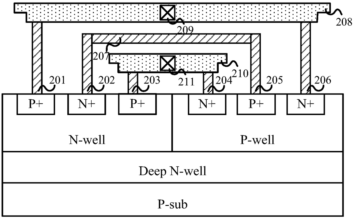
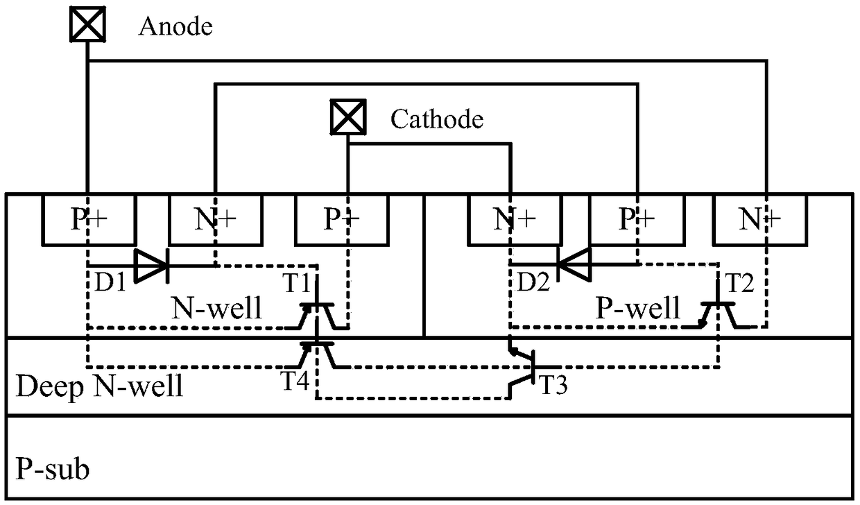
[0028] The invention designs a bidirectional transient voltage suppressor with diode string assisted triggering SCR by combining the characteristics of low and controllable diode string trigger voltage and strong robustness of SCR structure over-electric stress. The device of the present invention can form a current discharge path with strong robustness and no hysteresis under the action of positive and reverse electrical stresses, and realize bidirectional ESD or transient surge protection.
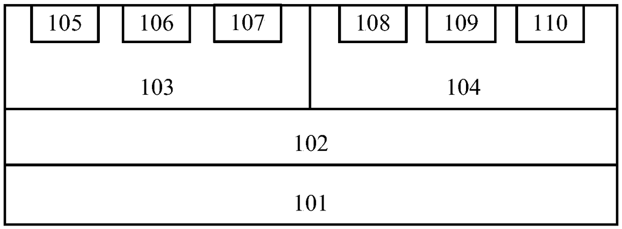
[0029] The bidirectional transient voltage suppressor provided by the present invention has a device structure profile such as figure 1 As shown, it is characterized in that it mainly includes a P substrate 101, a deep N well 102, an N well 103, a P well 104, a first P + implantation region 105, a first N + implantation region 106, a second P + implantation region 107, and a second N+ injection area 108, third P+ injection area 109, third N+ injection area 110 and metal lines;
[0030] Among them, a deep N well 102 is provided on the surface area of ​​the P substrate 101, the left edge of the P substrate 101 is connected to the left edge of the deep N well 102, and the right edge of the deep N well 102 is connected to the left edge of the P substrate 101. Connected to the right edge;
[0031] On the surface area of ​​the deep N well 102, an N well 103 and a P well 104 are sequentially arranged from left to right. The left edge of the deep N well 102 is connected to the left edge of the N well 103, and the right edge of the N well 103 is connected to the P The left edge of the well 104 is connected, and the right edge of the P well 104 is connected to the right edge of the deep N well 102;
[0032] A first P+ implantation region 105, a first N+ implantation region 106, and a second P+ implantation region 107 are sequentially provided on the surface area of ​​the N well 103 from left to right;
[0033] A second N+ implantation region 108, a third P+ implantation region 109, and a third N+ implantation region 110 are sequentially arranged on the surface area of ​​the P well 104 from left to right;
[0034] The metal wire is used to connect the injection area, and two electrodes are drawn from the metal wire as two electrical stress terminals.
[0035] The bidirectional transient voltage suppressor proposed by the present invention, the device metal connection is such as figure 2 As shown, the connection between the metal line and the injection zone is as follows: the first P+ injection zone 105 is connected to the first metal 201, the first N+ injection zone 106 is connected to the second metal 202, and the second P+ injection zone 107 is connected to the third metal. The metal 203 is connected, the second N+ injection region 108 is connected to the fourth metal 204, the third P+ injection region 109 is connected to the fifth metal 205, and the third N+ injection region 110 is connected to the sixth metal 206;
[0036] Both the second metal 202 and the fifth metal 205 are connected to the seventh metal 207;
[0037] The first metal 201 and the sixth metal 206 are both connected to the eighth metal 208, and the first electrode 209 is drawn from the eighth metal 208 to serve as the first electrical stress terminal of the device;
[0038] The third metal 203 and the fourth metal 204 are both connected to the ninth metal 210, and the second electrode 211 is drawn from the ninth metal 210 to serve as the second electrical stress terminal of the device.
[0039] The bidirectional transient voltage suppressor proposed by the present invention has an equivalent circuit under the action of forward electrical stress as image 3 As shown, when the first electrical stress terminal of the device is connected to a high potential and the second electrical stress terminal is grounded, the diode D1 is formed by the first P+ injection region 105 and the N well 103, and the diode D1 is formed by the P well 104 and the second N+ injection region 108 The diode D2, the diode D1 and the diode D2 form a first series path through the first N+ injection region 106, the metal line and the third P+ injection region 109. When the electrical stress reaches 1.4V, the first series path is opened. At the same time, the PNP tube T1 is composed of the first P+ injection region 105, the N well 103 and the second P+ injection region 107, and the NPN tube T2 is composed of the second N+ injection region 108, the P well 104 and the third N+ injection region 110. The NPN tube T3 composed of the N well 103, the P well 104 and the second N+ implanted region 108 and the PNP tube T4 composed of the first P+ implanted region 105, the N well 103 and the P well 104 all start to work in the amplified state, which can improve the device The current discharge capacity. The first SCR structure formed by the PNP tube T4 and the NPN tube T3 is beneficial to further enhance the robustness of the device.
[0040] The bidirectional transient voltage suppressor proposed by the present invention has an equivalent circuit under the action of reverse electrical stress as Figure 4 As shown, when the first electrical stress terminal of the device is grounded and the second electrical stress terminal is connected to a high potential, the diode D3 composed of the second P+ implanted region 107 and the N well 103 is composed of the P well 104 and the third N+ implanted region 110 A diode D4 is formed. The diode D3 and the diode D4 form a second series path through the first N+ injection region 106, the metal line, and the third P+ injection region 109. When the electrical stress reaches 1.4V, the second series path is opened. At the same time, the PNP tube T1 is composed of the first P+ injection region 105, the N well 103 and the second P+ injection region 107, and the NPN tube T2 is composed of the second N+ injection region 108, the P well 104 and the third N+ injection region 110. N-well 103, P-well 104 and the third N+ implanted region 110 constitute the NPN tube T5 and the second P+ implanted region 107, N-well 103 and P-well 104 constitute the PNP tube T6 are all started to work in the amplified state, can improve the device The current discharge capacity. Among them, the second SCR structure composed of PNP tube T5 and NPN tube T6 is beneficial to further enhance the robustness of the device.
[0041] The forward and reverse electrical stresses are applied between the first electrical stress terminal and the second electrical stress terminal, and the electrical characteristics of the device are the same. The two-way transient voltage suppressor that triggers the SCR assisted by the diode string has two-way electrostatic discharge protection or anti-wave Surge effect.
[0042] Finally, it should be noted that the above embodiments are only used to illustrate the technical solutions of the present invention and not to limit them. Although the present invention has been described in detail with reference to the preferred embodiments, those of ordinary skill in the art should understand that the technical solutions of the present invention can be implemented Modifications or equivalent replacements without departing from the purpose and scope of the technical solution of the present invention should be covered by the scope of the claims of the present invention.

PUM

no PUM

Description & Claims & Application Information

We can also present the details of the Description, Claims and Application information to help users get a comprehensive understanding of the technical details of the patent, such as background art, summary of invention, brief description of drawings, description of embodiments, and other original content. On the other hand, users can also determine the specific scope of protection of the technology through the list of claims; as well as understand the changes in the life cycle of the technology with the presentation of the patent timeline. Login to view more.

Similar technology patents

System and method for improving signaling channel robustness

ActiveUS20090164873A1improve robustnesshigh time diversity
Owner:SAMSUNG ELECTRONICS CO LTD

Complementary-type SCR (Silicon Controlled Rectifier) structure triggered by diode string in an auxiliary way

InactiveCN101771040ALower the trigger voltageWafer Area Reduction
Owner:ZHEJIANG UNIV

Classification and recommendation of technical efficacy words

  • Lower the trigger voltage
  • Improve robustness

Complementary-type SCR (Silicon Controlled Rectifier) structure triggered by diode string in an auxiliary way

InactiveCN101771040ALower the trigger voltageWafer Area Reduction
Owner:ZHEJIANG UNIV

Automatic parking method based on fusion of vision and ultrasonic perception

ActiveCN110775052AImprove robustnessImprove obstacle avoidance reliability
Owner:ZHEJIANG LEAPMOTOR TECH CO LTD

Finite time convergence time-varying sliding mode attitude control method

InactiveCN105242676AImprove robustnessEliminate jumping problems
Owner:BEIJING INSTITUTE OF TECHNOLOGYGY
Why Eureka
Try Eureka