OLED display panel and manufacturing method thereof and OLED display device

A display panel and display substrate technology, which is applied in semiconductor/solid-state device manufacturing, electrical components, electric solid-state devices, etc., can solve the problems of uneven display brightness and increased cathode resistance of OLED display panels

Active Publication Date: 2018-11-30
BOE TECH GRP CO LTD
View PDF5 Cites 10 Cited by
  • Summary
  • Abstract
  • Description
  • Claims
  • Application Information

AI Technical Summary

Problems solved by technology

[0004] The inventors found that in the existing bottom-emitting OLED, the deposition thickness of the cathode is reduced to have a certain transmittance, and the reduction of the thickness of the cathode will lead to an increase in the resistance of the cathode, thereby generating a large voltage drop (IR Drop), Make the display brightness of the OLED display panel uneven

Method used


Image

  • OLED display panel and manufacturing method thereof and OLED display device
  • OLED display panel and manufacturing method thereof and OLED display device
  • OLED display panel and manufacturing method thereof and OLED display device

Examples


Embodiment 1

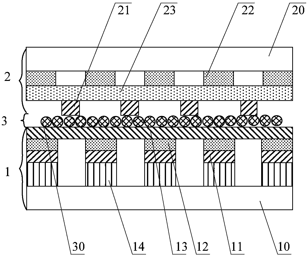
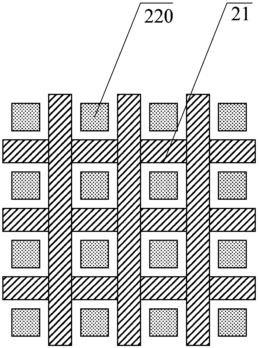
[0069] figure 1 Schematic structure of the OLED display panel provided for the embodiment of the present invention Figure 1 ,Such as figure 1 As shown, the OLED display panel provided by the embodiment of the present invention includes: an OLED display substrate 1 and an encapsulation substrate 2 arranged oppositely; the OLED display substrate 1 includes: a first substrate 10 and first electrodes 11 sequentially arranged on the first substrate , the organic light-emitting layer 12 and the second electrode 13; the encapsulation substrate 2 includes: a second substrate 20 and a conductive layer 21 arranged on the second substrate 20; the surface of the OLED display substrate 1 provided with the second electrode 13 is arranged with the encapsulation substrate 2 The surfaces with the conductive layer 21 are bonded by bonding glue 3 .

[0070] Wherein, the bonding glue 3 includes conductive particles 30 , and the conductive layer 21 is electrically connected to the second electr...

Embodiment 2

[0104] Based on the inventive concepts of the above embodiments, the embodiments of the present invention also provide a method for manufacturing an OLED display panel, Figure 7 The flow chart of the OLED display panel manufacturing method provided by the embodiment of the present invention, such as Figure 7As shown, the OLED display panel manufacturing method provided by the embodiment of the present invention specifically includes the following steps:

[0105] Step 100, providing a first substrate.

[0106] Optionally, the first substrate can be a rigid substrate or a flexible substrate, wherein the rigid substrate can be, but not limited to, one or more of glass and metal sheets; the flexible substrate can be, but not limited to, polyethylene terephthalate Glycol esters, ethylene terephthalate, polyether ether ketone, polystyrene, polycarbonate, polyarylate, polyarylate, polyimide, polyvinyl chloride, polyethylene, textile fibers one or more of.

[0107] Step 200, sequ...

Embodiment 3

[0132] Based on the inventive concepts of the above embodiments, the embodiments of the present invention further provide an OLED display device, and the OLED display device provided in the embodiments of the present invention includes: an OLED display panel.

[0133] Wherein, the OLED display panel is the OLED display panel provided in Embodiment 1, specifically a bottom-emitting OLED display panel, and its implementation principle and implementation effect are similar, and will not be repeated here.

[0134] Specifically, the display device may be any product or component with a display function such as a mobile phone, a tablet computer, a television, a monitor, a notebook computer, a digital photo frame, and a navigator, which is not limited in this embodiment of the present invention.

[0135] The drawings of the embodiments of the present invention only relate to the structures involved in the embodiments of the present invention, and other structures may refer to common d...


PUM


Abstract

The embodiment of the invention provides an OLED display panel and a manufacturing method thereof and an OLED display device. The OLED display panel includes an OLED display substrate and a packagingsubstrate which are arranged relatively. The OLED display substrate comprises a first substrate, a first electrode, a second electrode and an organic luminescence layer, wherein the first electrode, the second electrode and the organic luminescence layer are arranged in sequence on the first substrate. The packaging substrate comprises a second substrate and a conductive layer disposed on the second substrate. The surface provide with the second electrode of the OLED display substrate is bonded with surface provided with the conductive layer of the packaging substrate through bonding adhesive,wherein the bonding adhesive includes conductive particles. The conductive layer is electrically connected with the second electrode by the conducting particles. The OLED display panel and the manufacturing method thereof and the OLED display device enable the conductive layer and the second electrode to be electrically connected by including the conductive particles in the bonding adhesive, theentire electrode layer includes the conductive layer and the second electrode, the resistance of the entire electrode layer is reduced, the voltage drop is reduced, and the brightness uniformity of the OLED display panel is ensured.

Description

technical field [0001] Embodiments of the present invention relate to the field of display technology, and in particular to an OLED display panel, a manufacturing method thereof, and an OLED display device. Background technique [0002] Organic light-emitting diode (Organic Light-Emitting Device, referred to as OLED) display panel is a display device different from traditional liquid crystal display (Liquid Crystal Display, referred to as LCD), with active light, good temperature characteristics, low power consumption, responsive Fast, bendable, ultra-thin and low cost. Therefore, it has become one of the important development discoveries of the new generation display device, and has received more and more attention. [0003] OLED display panels can be divided into three types according to the direction of light emission: bottom-emitting OLEDs, top-emitting OLEDs, and double-sided emitting OLEDs. Wherein, the bottom emission OLED includes: an encapsulation substrate and an...

Claims


Application Information

Patent Timeline
Patent Type & Authority Applications(China)
IPC IPC(8): H01L27/32H01L51/52H01L51/56
CPCH10K59/1315H10K50/841H10K71/00H01L2224/83851H01L2224/32225H01L2224/9211H01L2224/81903H10K59/13H01L2224/81H01L2224/83H01L24/05H01L24/32H01L25/18H01L25/50H01L2224/05623H01L2224/05624H01L2224/05639
Inventor 丁小梁董学王海生陈小川邓立凯
Owner BOE TECH GRP CO LTD
Why Eureka
Try Eureka