Semiconductor structure and formation method thereof

A technology of semiconductor and isolation structure, applied in the field of semiconductor structure and its formation, can solve the problems of poor performance of semiconductor structure and poor isolation performance of isolation structure, and achieve the effect of improving performance

Inactive Publication Date: 2018-12-07
SEMICON MFG INT (SHANGHAI) CORP +1
View PDF4 Cites 0 Cited by
  • Summary
  • Abstract
  • Description
  • Claims
  • Application Information

AI Technical Summary

Problems solved by technology

[0005] However, the existing solid source doping process easily leads to poor isolation performance of the formed fin field effect transistor isolation structure, and poor performance of the semiconductor structure.

Method used


Image

  • Semiconductor structure and formation method thereof
  • Semiconductor structure and formation method thereof
  • Semiconductor structure and formation method thereof

Examples


Embodiment Construction

[0032] There are many problems in the formation method of the semiconductor structure, for example: the formation method of the semiconductor structure may easily cause poor isolation performance of the isolation structure in the semiconductor structure, which affects the performance of the semiconductor structure.

[0033] In combination with a method for forming a semiconductor structure, the reasons for the poor isolation performance of the isolation structure in the semiconductor structure are analyzed:

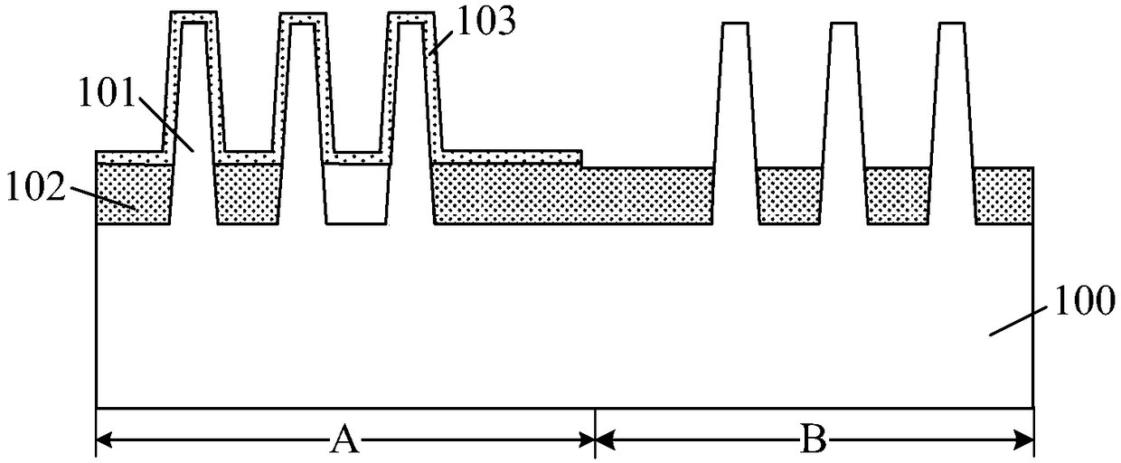
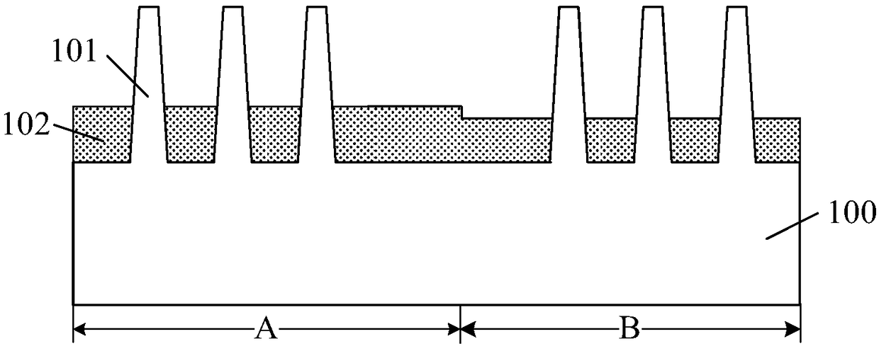
[0034] figure 1 and figure 2 It is a structural schematic diagram of each step of a method for forming a semiconductor structure.

[0035] Please refer to figure 1 , providing a substrate, the substrate includes a first region A and a second region B; the substrate includes: a substrate 100, a fin 101 located on the substrate 100; an isolation structure 102 is provided on the substrate; The first region A has a doped layer 103 on the substrate, and the doped layer 1...


PUM

PropertyMeasurementUnit
thicknessaaaaaaaaaa
thicknessaaaaaaaaaa

Abstract

The invention provides a semiconductor structure and a formation method thereof. The method comprises the following steps: providing a substrate, wherein the substrate comprises a first region and a second region, and the substrate has an isolation structure; forming a protection layer on the second region substrate and the second region isolation structure; forming a doping layer on the first region substrate, the first region isolation structure and the protection layer; carrying out annealing treatment on the doping layer to enable doping ions in the doping layer to diffuse into the first region substrate to form a first doped region; and after carrying out annealing treatment on the doping layer, removing the doping layer. The method enables the performance of the semiconductor structure to be good, and the formation process of the semiconductor structure is simple.

Description

technical field [0001] The invention relates to the technical field of semiconductor manufacturing, in particular to a semiconductor structure and a forming method thereof. Background technique [0002] With the improvement of the integration level of semiconductor devices, the critical dimensions of transistors are continuously reduced, and the width of the gate structure is also reduced, so that the length of the channel under the gate structure is continuously reduced. The reduction of the channel length in the transistor increases the possibility of charge punching between the source and drain doped regions, and easily causes channel leakage current. [0003] The gate of the Fin Field-Effect Transistor (FinFET) has a forked 3D structure similar to a fish fin. The channel of the FinFET protrudes from the surface of the substrate to form a fin, and the gate covers the top surface and side walls of the fin, which can control the on and off of the circuit on both sides of t...

Claims


Application Information

Patent Timeline
Patent Type & Authority Applications(China)
IPC IPC(8): H01L21/336H01L29/06H01L29/78
CPCH01L29/0638H01L29/0653H01L29/66795H01L29/785H01L21/2255H01L21/76229H01L21/823807H01L21/823821H01L21/823878H01L27/0924H01L29/66803H01L29/7853H01L21/0214H01L21/0217H01L21/02271H01L21/0228H01L21/26513H01L21/31053H01L21/31116H01L21/324H01L21/76224H01L21/823814H01L21/823864H01L29/0649H01L29/0847H01L29/167H01L29/36H01L29/6656
Inventor 周飞
Owner SEMICON MFG INT (SHANGHAI) CORP
Why Eureka
Try Eureka