Server chip debugging circuit, debugging method and server

A technology for debugging circuits and debugging methods, which is applied in the direction of faulty hardware testing methods, instruments, and electrical digital data processing, etc., which can solve the problems of increased manufacturing costs, cumbersome operations, and high costs of servers, and achieve improved space utilization, reduced costs, and Effect of saving board space

Inactive Publication Date: 2018-12-11
ZHENGZHOU YUNHAI INFORMATION TECH CO LTD
View PDF5 Cites 9 Cited by
  • Summary
  • Abstract
  • Description
  • Claims
  • Application Information

AI Technical Summary

Problems solved by technology

[0003] The server is equipped with multiple debug connectors, and the high cost of multiple debug connectors will also increase the manufacturing cost of the server
When debugging different chips, it is necessary to manually connect to the corresponding debugging connector, which is cumbersome to operate

Method used


Image

  • Server chip debugging circuit, debugging method and server
  • Server chip debugging circuit, debugging method and server

Examples


Embodiment 1

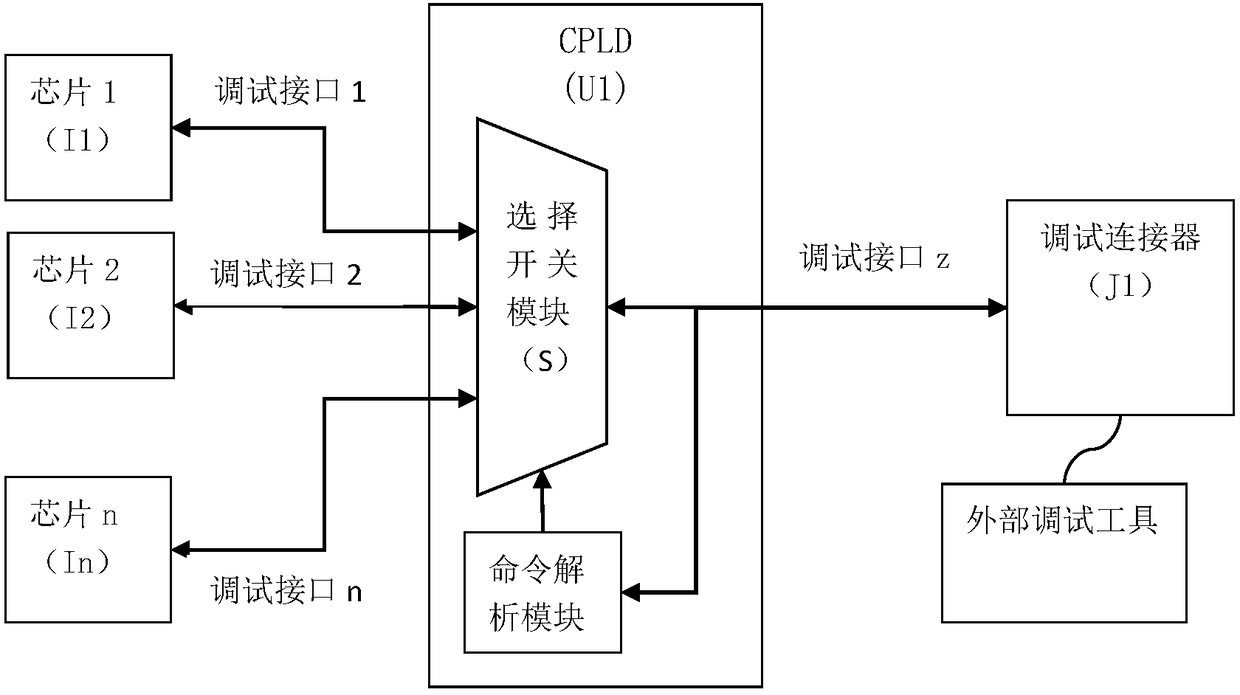
[0022] Such as figure 1 As shown, a server chip debugging circuit includes: a debugging control unit U1, n chips to be debugged (I1, I2, . . . , In) and a debugging connector J1. In this embodiment, the debugging control unit is specifically a CPLD chip.

[0023] The debugging control unit includes a selection switch module S and a command analysis module. One end of the selection switch module is respectively connected to the debugging interfaces (debugging interface 1, debugging interface 2, . . . , debugging interface n) of the plurality of debugged chips through the first interface. In this embodiment, the debugging interface 1, the debugging interface 2, . . . , the debugging interface n, and the debugging interface z are specifically I2C protocol interfaces.

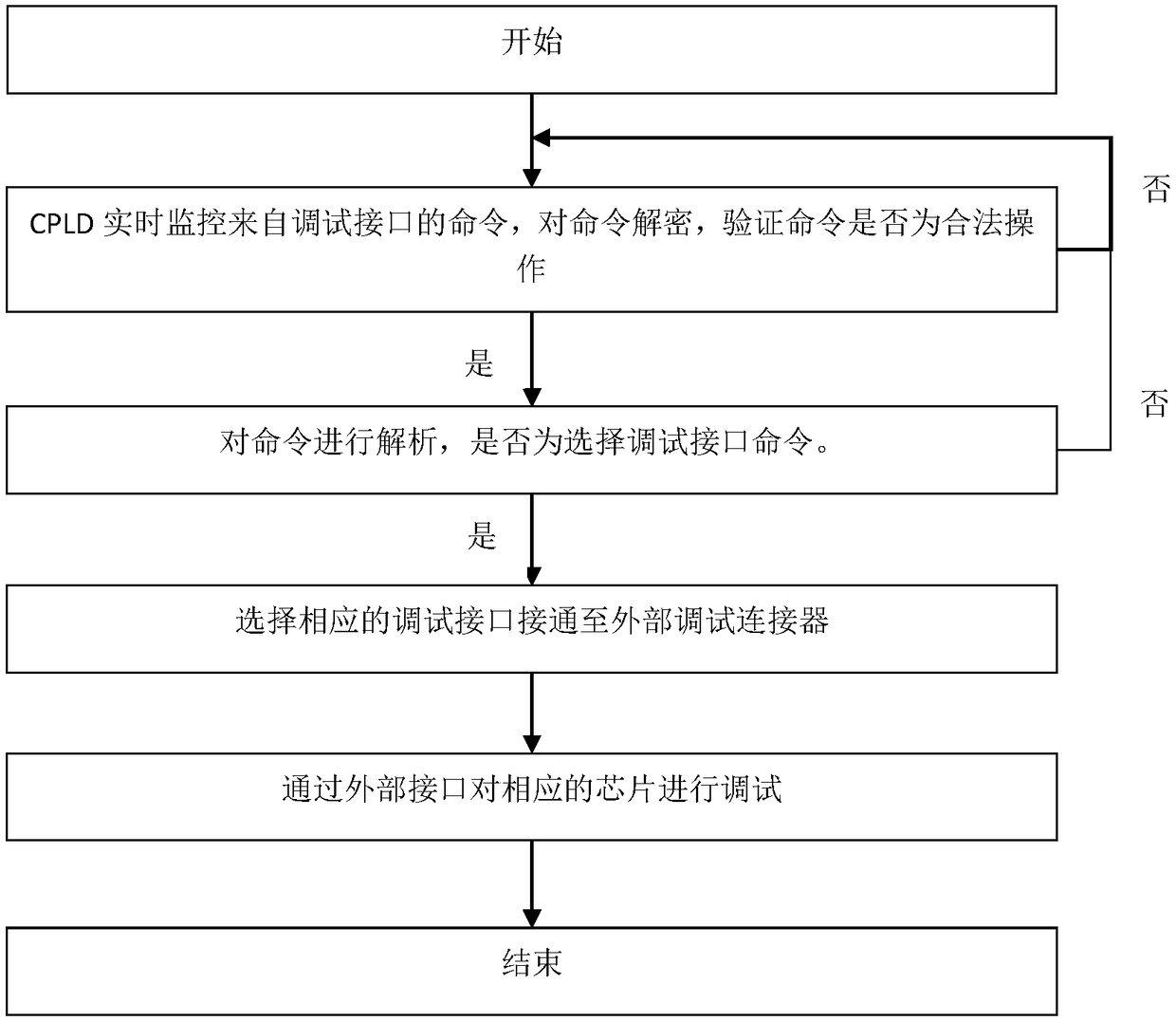
[0024] The other end of the selection switch module is connected to the debugging connector through the debugging interface z. The command parsing module is used for accepting the commands of the debugging inter...

Embodiment 2

[0029] The difference between this embodiment and Embodiment 1 is that in this embodiment, the debugging interface 1, the debugging interface 2, . . . , the debugging interface n are I2C protocol interfaces. The debugging interface z is a UART protocol interface. The debugging control unit includes a protocol conversion module, which realizes the conversion between the I2C protocol interface and the UART protocol interface of the debugging interface z. Through the protocol conversion module, the optional range of protocols on both sides of the debugging control unit is increased.


PUM


Abstract

The embodiment of the invention discloses a server chip debugging circuit, a debugging method and a server, belonging to the server design field. The debugging circuit comprises a debugging control unit, a plurality of chips to be debugged and a debugging connector. The debugging control unit comprises a selector switch module and a command parsing module. One end of the selective switch module isconnected with the debugging interface of the plurality of chips to be debugged through the first interface, and the other end of the selective switch module is connected with the debugging connector. The command parsing module is used for receiving the command of the debugging interface and controlling the selection switch module to select and turn on a chip to be debugged and a debugging connector according to the command. The debugging control unit switches the debugging interfaces of a plurality of chips to the connectors of a debugging interface, and can flexibly switch each interface through commands according to requirements, thereby saving circuit board space, reducing cost, improving debugging flexibility, and providing an effective method for improving the utilization rate of server board space.

Description

technical field [0001] The invention relates to the field of server circuit design. Background technique [0002] With the rapid development of servers, the server has more and more functions and stronger performance, which also leads to the continuous increase of devices on the circuit board. How to lay out more functional chips in the limited circuit board space has become a problem of A difficulty of design. In the server system, there are many kinds of chip interfaces, and it is necessary to reserve debugging interfaces for multiple chips to facilitate system debugging and maintenance. When the server is running normally, the utilization rate of these debugging interfaces is low, and multiple debugging interface connectors also occupy more circuit board space. [0003] The server is provided with multiple debugging connectors, and the high cost of the multiple debugging connectors also increases the manufacturing cost of the server. When debugging different chips, it ...

Claims


Application Information

Patent Timeline
Patent Type & Authority Applications(China)
IPC IPC(8): G06F11/22G06F13/40
CPCG06F11/2236G06F11/2273G06F11/2284G06F13/4022
Inventor 董超刘栋
Owner ZHENGZHOU YUNHAI INFORMATION TECH CO LTD
Why Eureka
Try Eureka