Pixel structure

A technology of pixel structure and pixel driving circuit, which is applied in the field of pixel structure, can solve the problems of large leakage current of thin film transistors, easy occurrence of bright spots on the display panel, and influence on the compensation effect of 7T1C circuits, and achieve the effect of increasing the effective channel length

Active Publication Date: 2018-12-14
WUHAN CHINA STAR OPTOELECTRONICS SEMICON DISPLAY TECH CO LTD
View PDF12 Cites 7 Cited by
  • Summary
  • Abstract
  • Description
  • Claims
  • Application Information

AI Technical Summary

Problems solved by technology

[0009] An embodiment of the present invention provides a pixel structure and an array substrate; in order to solve the problem that in the pixel structure of the existing 7T1C circuit, the channel length of the thin film transistor is relatively short, and the device width-to-length ratio W / L is relatively large, which leads to the leakage of the thin film transistor. The current is relatively large, which affects the compensation effect of the 7T1C circuit, resulting in a technical problem that the display panel is prone to bright spots when the screen is black

Method used


Image

  • Pixel structure
  • Pixel structure
  • Pixel structure

Examples


Embodiment Construction

[0042] Please refer to the drawings in the accompanying drawings, wherein like reference numerals refer to like components. The following description is based on illustrated specific embodiments of the invention, which should not be construed as limiting other specific embodiments of the invention not described in detail herein.

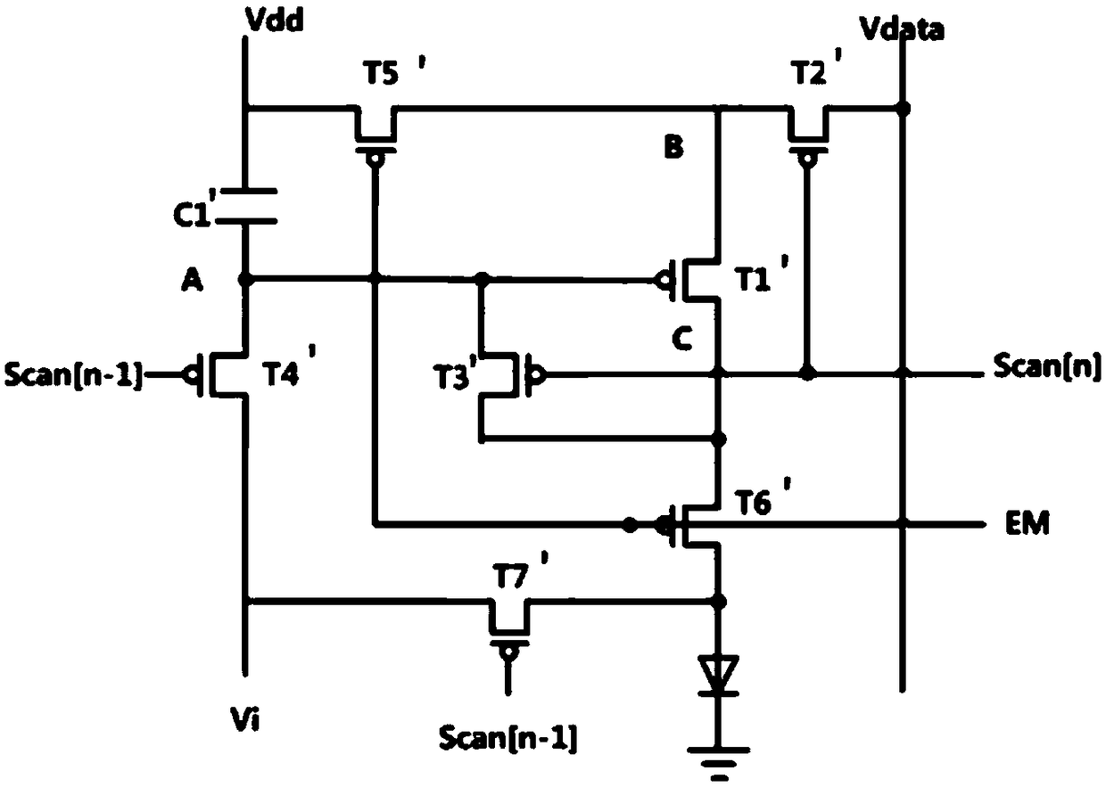
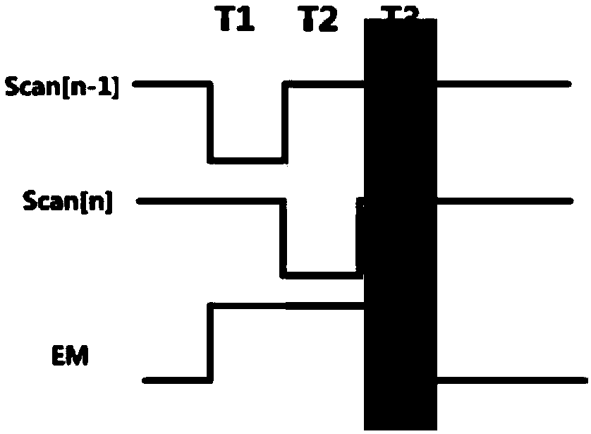
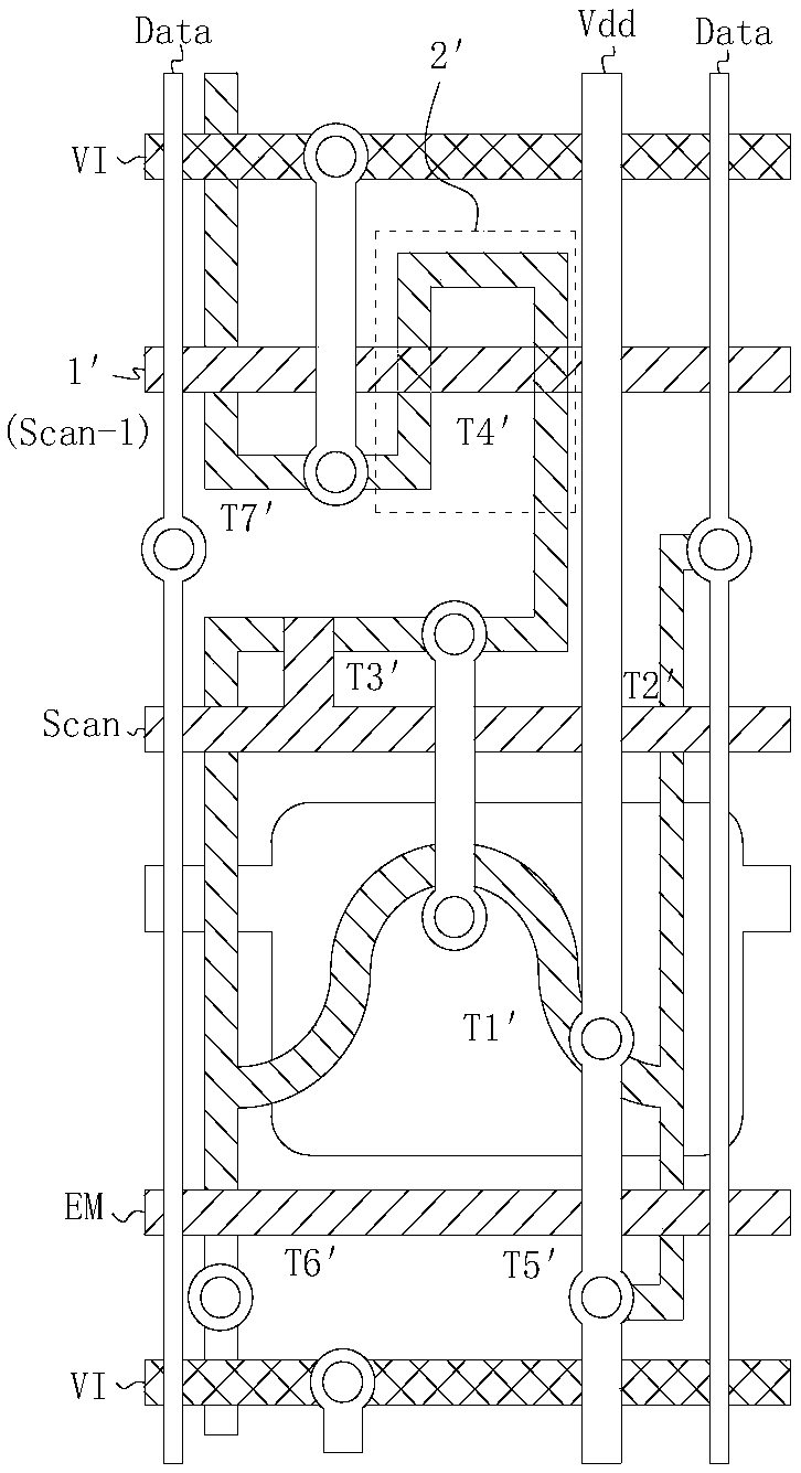
[0043] Please refer to Figure 4 and Figure 5 , Figure 4 It is a structural schematic diagram of the first embodiment of the pixel structure of the present invention; Figure 5 It is a structural schematic diagram of the scanning line and the thin film transistor of the first embodiment of the pixel structure of the present invention. It should be noted that the pixel structure of the first embodiment of the present invention is used in the pixel driving circuit of 7T1C, and the equivalent circuit and driving timing of the 7T1C pixel driving circuit of the present invention are consistent with those of the prior art.

[0044] The pixel driving ...


PUM


Abstract

The invention provides a pixel structure comprising a thin film transistor having a first gate electrode and a second gate electrode and an active layer having a first strip part and a second strip part. The first gate electrode is inclined in the extending direction of the orthogonal projection on the plane of the active layer and the extending direction of the first strip part. The second gate electrode is inclined in the extending direction of the orthogonal projection on the plane of the active layer and the extending direction of the second strip part. The first gate electrode and the first strip part of the active layer are obliquely overlapped and the second gate electrode and the second strip part of the active layer are obliquely overlapped so that the effective channel length ofthe channel region of the thin film transistor can be enhanced.

Description

technical field [0001] The present invention relates to the field of display technology, in particular to a pixel structure. Background technique [0002] In the display area of ​​the AMOLED display device, the pixels are arranged in a matrix including multiple rows and columns, and usually each pixel is usually composed of two thin film transistors and a capacitor, commonly known as 2T1C circuit. This 2T1C design is very sensitive to the following factors: threshold voltage (Vth) and channel mobility (Mobility) of TFT, start-up voltage and quantum efficiency of OLED, and transient process of power supply. Therefore, compensation circuits are generally used to reduce the impact, such as 7T1C, 6T1C, 6T2C, etc. [0003] In the structure of the 7T1C pixel drive circuit, please refer to figure 1 with figure 2 , the thin film transistor T4' is used to control the discharge of the capacitor, the gate of the thin film transistor T4' is connected to the scanning line Scan[n-1], ...

Claims


Application Information

Patent Timeline
Patent Type & Authority Applications(China)
IPC IPC(8): G09G3/3266G09G3/3225
CPCG09G3/3225G09G3/3266
Inventor 马伟欣王少波陈彩琴
Owner WUHAN CHINA STAR OPTOELECTRONICS SEMICON DISPLAY TECH CO LTD
Why Eureka
Try Eureka