
Patsnap Eureka
For R&D, Patsnap Eureka makes reading and utilizing patents & technical documents easy.
Patsnap Eureka AIR
Designed for self-driven R&D workflows. Generate viable solutions, solve complex R&D challenges, empower your innovation with AI.

Patsnap Eureka Materials
Designed for material experts only. Revolutionize your material R&D, from search, analyze, to developing new materials.

TechResearch
Generate reliable direction feasibility study reports for your R&D in just a few steps.

TechSeek
Discover and master advanced knowledge NOW. Basics, ideas, possibilities, all at once.

TechMind
As an expert in R&D Theories, TechMind can generates customized viable solutions instantly.

TechRisk
Analyze your overall solution with one click, know your potential R&D risks in advance.

TechMonitor
Get weekly tech updates, stay abreast of the latest tech innovations and key insights.
Semiconductor structure and forming method thereof, forming method of fin-type field effect transistor
A semiconductor and isolation structure technology, applied in semiconductor devices, semiconductor/solid-state device manufacturing, electrical components, etc., can solve problems such as easy bridging, reduce the probability of gaps, improve electrical performance and yield, and reduce bridging problems.
- Summary
- Abstract
- Description
- Claims
- Application Information
AI Technical Summary
Problems solved by technology
Method used
Image

Examples
Embodiment Construction
[0019] It can be seen from the background art that the fin field effect transistor introduced with the stress layer in the prior art is prone to bridging problems. Now combine the formation method of a semiconductor structure to analyze the cause of its bridging problem:
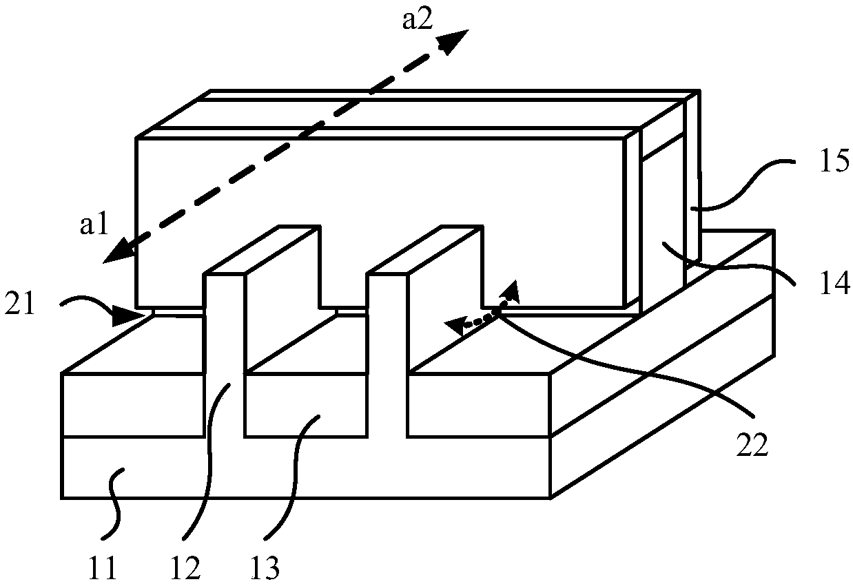
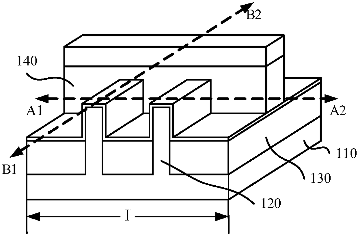
[0020] refer to Figure 1 to Figure 2 , shows a structural schematic diagram corresponding to each step in a method for forming a semiconductor structure.
[0021] refer to figure 1 , providing a substrate 11 with discrete fins 12 on the substrate 11; forming an isolation structure 13 on the substrate 11 exposed by the fins 12; forming an isolation structure 13 on the fins 12 and the isolation structure 13 A dummy gate structure 14 across the fin 12 , the dummy gate structure 14 covers part of the top and part of the sidewall surface of the fin 12 ; sidewalls 15 are formed on the sidewall of the dummy gate structure 14 .
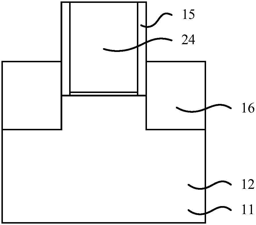
[0022] combined reference figure 2 , figure 2 yes figure 1 A schematic diagra...
PUM
 Abstract
Description
Claims
Application Information
 - R&D Engineer
- R&D Manager
- IP Professional
- Industry Leading Data Capabilities
- Powerful AI technology
- Patent DNA Extraction
Browse by: Latest US Patents, China's latest patents, Technical Efficacy Thesaurus, Application Domain, Technology Topic, Popular Technical Reports.
© 2024 PatSnap. All rights reserved.Legal|Privacy policy|Modern Slavery Act Transparency Statement|Sitemap|About US| Contact US: help@patsnap.com