Array substrate detection method and detection device

The technology of an array substrate and a detection method is applied in the field of an array substrate detection method and a detection device, which can solve the problem of long time consumption, and achieve the effects of reducing the detection time, improving the detection rate, and improving the product yield rate.

Active Publication Date: 2021-10-26
BOE TECH GRP CO LTD +1
View PDF29 Cites 0 Cited by
  • Summary
  • Abstract
  • Description
  • Claims
  • Application Information

AI Technical Summary

Problems solved by technology

[0006] Embodiments of the present invention provide an array substrate inspection method and inspection device, which are used to improve the time-consuming process of performing yield test on signal lines on an array substrate in the prior art

Method used


Image

  • Array substrate detection method and detection device
  • Array substrate detection method and detection device
  • Array substrate detection method and detection device

Examples


Embodiment Construction

[0029] The following will clearly and completely describe the technical solutions in the embodiments of the present invention with reference to the accompanying drawings in the embodiments of the present invention. Obviously, the described embodiments are only some, not all, embodiments of the present invention. Based on the embodiments of the present invention, all other embodiments obtained by persons of ordinary skill in the art without making creative efforts belong to the protection scope of the present invention.

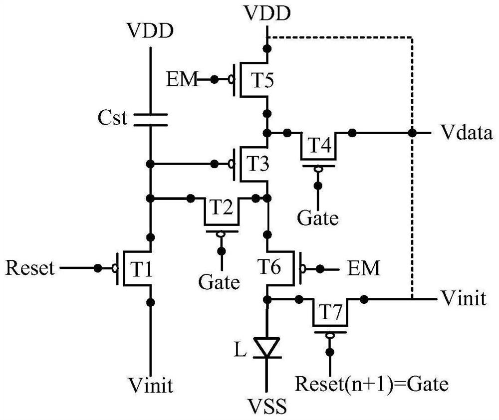
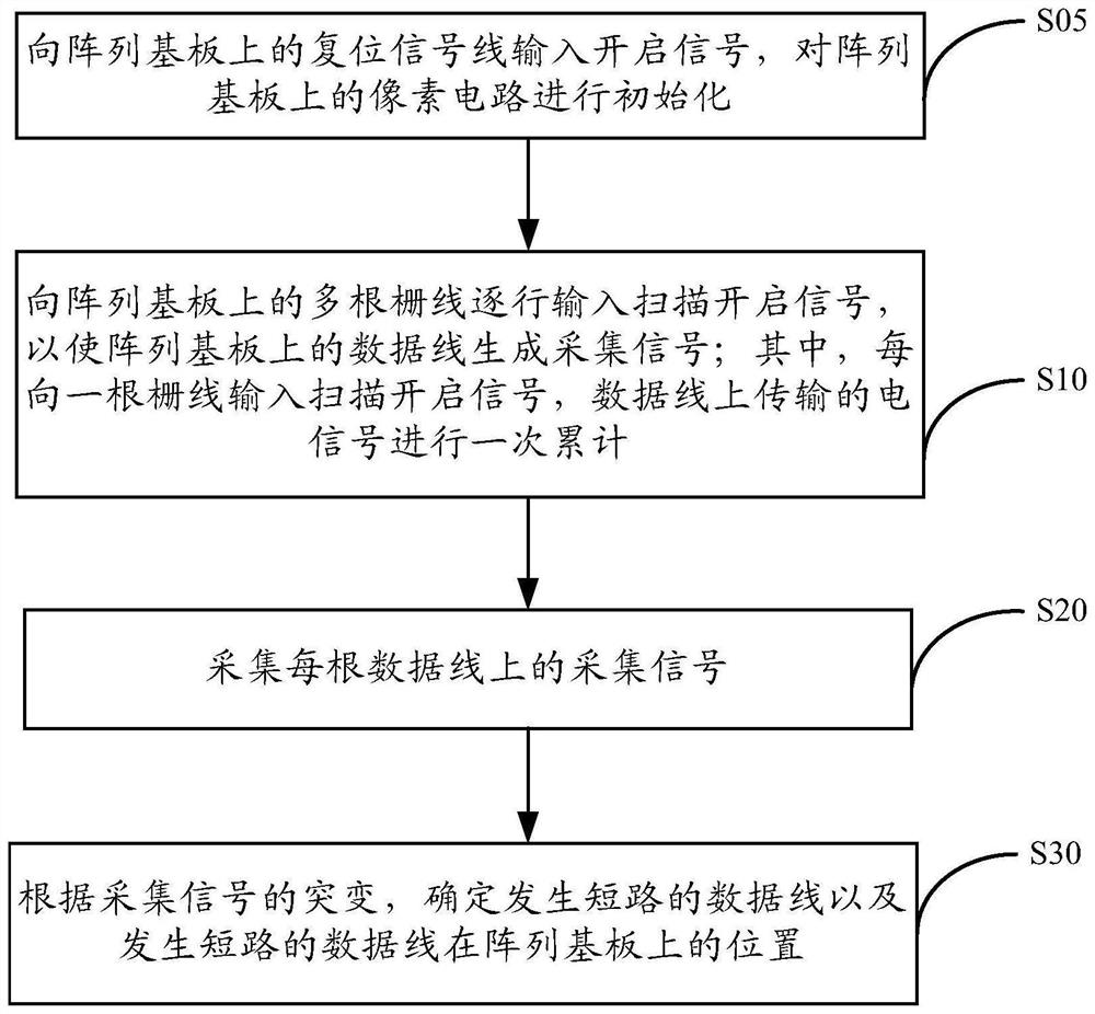
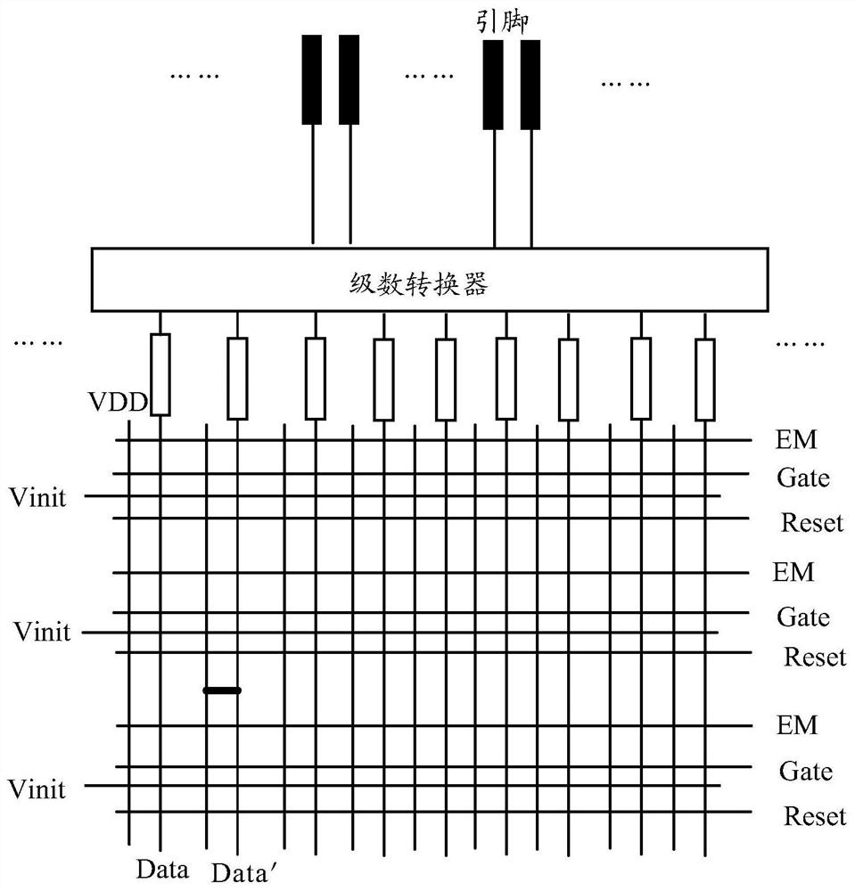
[0030] Taking the OLED display panel as an example, in the array process of the display panel, process errors inevitably occur, resulting in defective dots or lines on the array substrate. Among them, those skilled in the art can eliminate the problem of display defects caused by dot defects by performing aging treatment on the array substrate, thereby reducing the problem of dot defects on the array substrate. However, the Aging process cannot solve the probl...


PUM


Abstract

The invention provides an array substrate detection method and detection device, which relate to the field of display technology and are used to improve the time-consuming process of the yield test of signal lines on the array substrate in the prior art. The method for detecting an array substrate includes: inputting scan-on signals row by row to multiple gate lines on the array substrate, so that data lines on the array substrate generate acquisition signals; Signal, the electrical signal transmitted on the data line is accumulated once; the acquisition signal on each of the data lines is obtained; according to the sudden change of the acquisition signal, the short-circuited data line and the short-circuited data are determined The position of the line on the array substrate.

Description

technical field [0001] The present invention relates to the field of display technology, in particular to an array substrate detection method and a detection device. Background technique [0002] Commonly used display panels in the field of display technologies include OLED (Organic Light-Emitting Diode, organic electroluminescent diode) display panels and LCD (Liquid Crystal Display, liquid crystal display panels). [0003] Taking the OLED display panel as an example, the OLED display panel has the advantages of thinness, lightness, wide viewing angle, active luminescence, continuously adjustable luminous color, low cost, high color gamut, high contrast, fast response speed, low power consumption, low driving voltage, and excellent performance. It has the advantages of wide temperature range, simple production process, high luminous efficiency and flexible display. [0004] In the Array (array) process of the OLED display panel, the AT (Array Tester, Array Detector) will c...

Claims


Application Information

Patent Timeline
Patent Type & Authority Patents(China)
IPC IPC(8): G09G3/00
CPCG09G3/006
Inventor 李波李建楠王雷胡岩袁洪光刘备唐毅
Owner BOE TECH GRP CO LTD
Why Eureka
Try Eureka