Power device and encapsulation method thereof

A technology of power devices and packaging methods, which is applied in the direction of electric solid-state devices, semiconductor devices, semiconductor/solid-state device components, etc., can solve the problems of low thermal diffusion efficiency of chips, increase of manufacturing costs, and product failure, so as to reduce manufacturing costs, Improved integration and better packaging

Inactive Publication Date: 2018-12-18
SHENGSHIYAOLAN SHENZHEN TECH CO LTD
View PDF3 Cites 5 Cited by
  • Summary
  • Abstract
  • Description
  • Claims
  • Application Information

AI Technical Summary

Problems solved by technology

[0002] At present, power chips can have good electrical and thermal performance and work reliability, which lead to more and more high temperature or temperature drift of the chip during use. High temperature has a great impact on the reliability and rapid aging of power electronic products. Great impact, and excessive temperature and temperature cycle often directly lead to premature failure of the product
[0003] The traditional power chip package is directly soldered to the copper-clad ceramic substrate, and then the copper-clad ceramic substrate with the chip attached is connected to the heat sink. This package is called single-sided package. The heat dissipation channel of the single-sided package is mainly generated by the chip. The heat is transferred to the copper-clad ceramic substrate through the adhesive layer, and then transferred to the heat sink through another adhesive layer. Finally, the heat sink and air convection heat transfer or water cooling will dissipate the heat. However, the heat transfer direction in the single-sided package is determined by One-way transmission from the chip to the heat sink, although the overall heat dissipation capacity of the structure can be increased by using a connection material with a higher thermal conductivity or designing a heat sink with better heat dissipation capacity, resulting in low thermal diffusion efficiency of the chip, without increasing the chip area In the case of , if the heat dissipation layer is added, the manufacturing cost will also increase

Method used


Image

  • Power device and encapsulation method thereof
  • Power device and encapsulation method thereof
  • Power device and encapsulation method thereof

Examples


Embodiment Construction

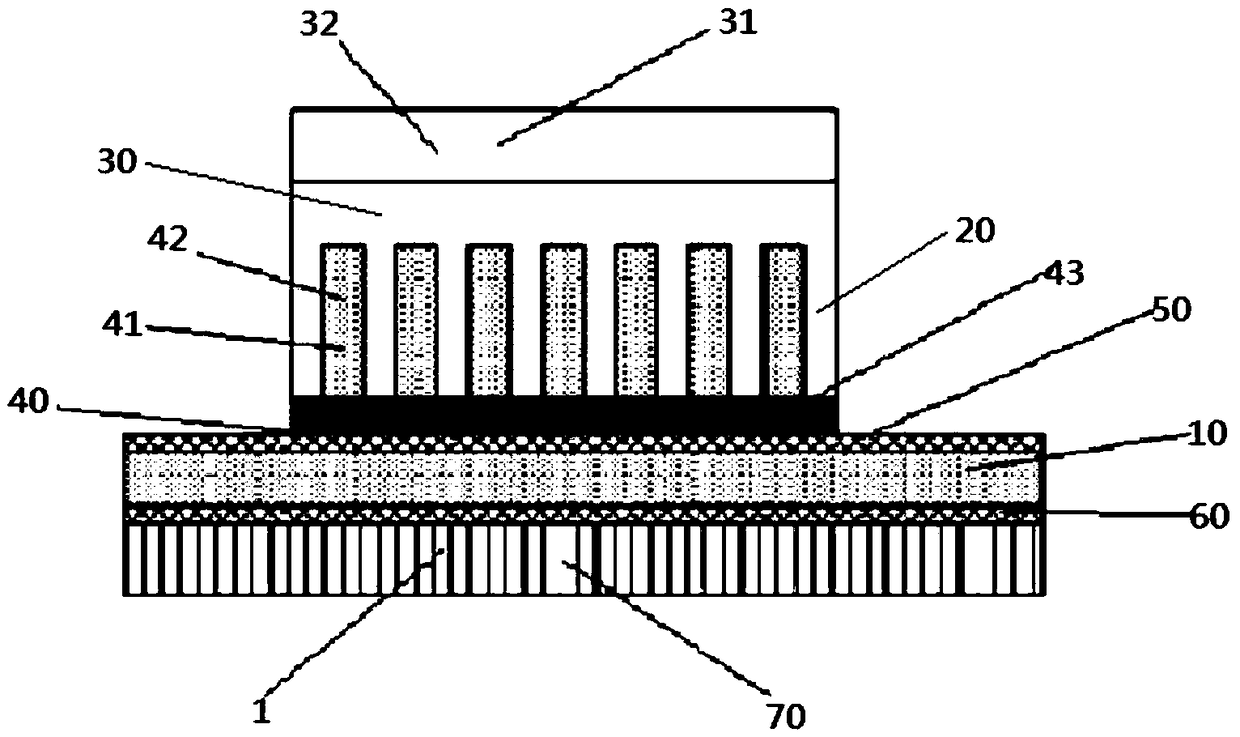
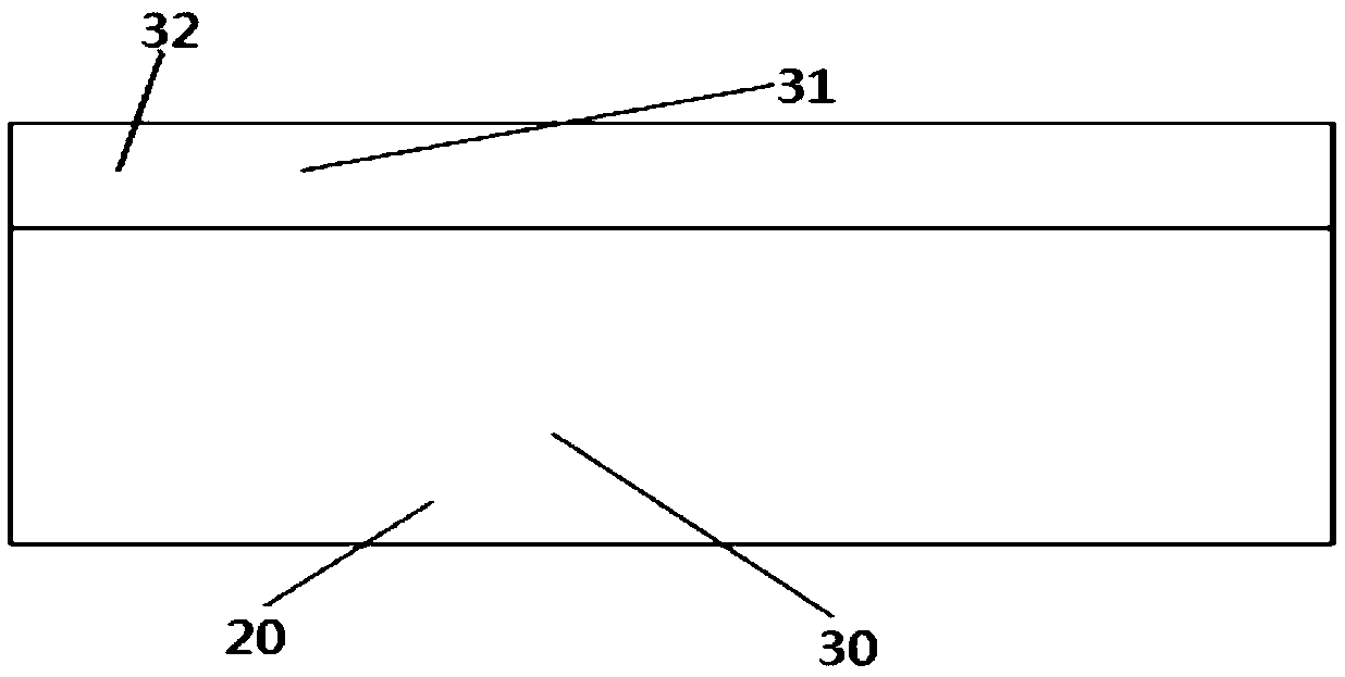
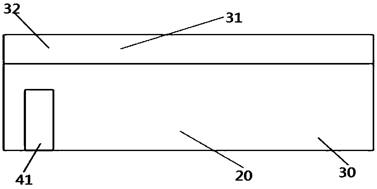
[0020] In order to understand the specific technical solutions, features and advantages of the present invention more clearly, the present invention will be further described in detail below in conjunction with the accompanying drawings and specific embodiments.

[0021] In the description of the present invention, it should be noted that the terms "upper", "lower", "left", "right", "transverse", "longitudinal", "horizontal", "inner", "outer" etc. indicate The orientation or positional relationship is based on the orientation or positional relationship shown in the drawings, or the orientation or positional relationship that is usually placed when the product of the invention is used, and is only for the convenience of describing the present invention and simplifying the description, rather than indicating or implying the It should not be construed as limiting the invention that a device or element must have a particular orientation, be constructed, and operate in a particular ...


PUM


Abstract

A power device is provided, which comprises a substrate and a chip arranged on the substrate, the chip includes a substrate and a heat conduction assembly formed on the substrate, the heat conductionassembly includes a plurality of grooves spaced apart on a lower surface of the substrate, a first metal layer formed in the trench, a second metal layer connected to the substrate on the substrate, the depth of the trench being smaller than the thickness of the substrate, and both the first metal layer and the second metal layer being in ohmic contact with the substrate. The invention also provides a packaging method of a power device, which enhances the heat dissipation efficiency and the driving performance of the chip, reduces the size of the chip after packaging, and reduces the manufacturing cost.

Description

technical field [0001] The invention relates to the technical field of power semiconductor chip packaging technology, in particular to a power device and a packaging method thereof. Background technique [0002] At present, power chips can have good electrical and thermal performance and work reliability, which lead to more and more high temperature or temperature drift of the chip during use. High temperature has a great impact on the reliability and rapid aging of power electronic products. Large impact, and excessive temperature and temperature cycle often directly lead to premature failure of the product. [0003] The traditional power chip package is directly soldered to the copper-clad ceramic substrate, and then the copper-clad ceramic substrate with the chip attached is connected to the heat sink. This package is called single-sided package. The heat dissipation channel of the single-sided package is mainly generated by the chip. The heat is transferred to the coppe...

Claims


Application Information

Patent Timeline
Patent Type & Authority Applications(China)
IPC IPC(8): H01L23/373H01L23/367H01L29/45
CPCH01L23/367H01L23/3736H01L29/456
Inventor 郑琼如
Owner SHENGSHIYAOLAN SHENZHEN TECH CO LTD
Why Eureka
Try Eureka