Surge protection chip and preparation method thereof

A surge protection and chip technology, applied in the direction of electrical components, diodes, electric solid devices, etc., can solve the problems of reducing the performance of surge protection chips, high-frequency circuit signals are easily interfered, and it is difficult to protect sensitive circuits. Surge protection capability, reduction of discharge density, effect of increasing chip area

Pending Publication Date: 2021-11-23
安芯半导体技术(深圳)有限公司
View PDF0 Cites 0 Cited by
  • Summary
  • Abstract
  • Description
  • Claims
  • Application Information

AI Technical Summary

Problems solved by technology

Various voltage surges from electrostatic discharge to lightning can induce transient current spikes, which makes it difficult for the surge discharge path of the surge protection chip and its own clamping voltage to protect sensitive circuits from surges. Electrostatic discharge and other transient voltages that appear randomly in the form of voltage surges usually exist in the device, making high-frequency circuit signals susceptible to interference and reducing the performance of surge protection chips

Method used


Image

  • Surge protection chip and preparation method thereof
  • Surge protection chip and preparation method thereof
  • Surge protection chip and preparation method thereof

Examples


preparation example Construction

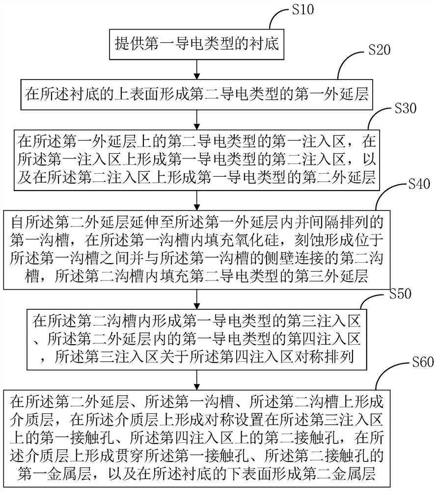
[0039] refer to figure 1 , Figure 2 to Figure 10 , the present invention also provides a preparation method of a surge protection chip, comprising the following steps:

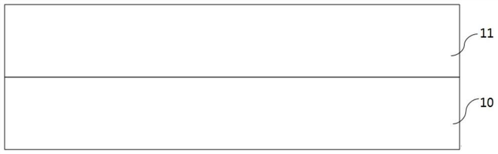
[0040] S10: providing a substrate 10 of a first conductivity type;

[0041] S20: forming a first epitaxial layer 11 of a second conductivity type on the upper surface of the substrate 10;

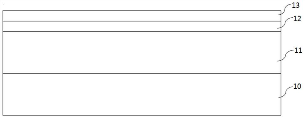
[0042] S30: a first implantation region 12 of the second conductivity type is formed on the first epitaxial layer 11, a second implantation region 13 of the first conductivity type is formed on the first injection region 12, and a second implantation region 13 of the first conductivity type is formed on the second forming a second epitaxial layer 14 of the first conductivity type on the implantation region 13;

[0043] S40: Extending from the second epitaxial layer 14 to the first epitaxial layer 11 and spaced apart first trenches 15, filling the first trenches 15 with silicon oxide 16, etching and forming A second tre...


PUM


Abstract

The invention discloses a surge protection chip which comprises a substrate, a first epitaxial layer formed on the substrate, a first injection region on the first epitaxial layer, a second injection region on the first injection region, a second epitaxial layer on the second injection region, first grooves extending into the first epitaxial layer from the second epitaxial layer, and silicon oxide filled in the first groove, second grooves located between the first grooves and connected with the side walls of the first grooves, third epitaxial layer filled in the second grooves, a third injection region formed in the second grooves, a fourth injection region formed in the second epitaxial layer, a dielectric layer formed on the second epitaxial layer, the first grooves and the second grooves, a first contact hole formed in the dielectric layer and correspondingly formed in the third injection region, a second contact hole formed in the fourth injection region, a first metal layer arranged on the dielectric layer and filling the first contact hole and the second contact hole, and a second metal layer formed under the substrate. The invention further provides a preparation method of the surge protection chip, and the parasitic capacitance and high-frequency circuit signal attenuation are reduced.

Description

technical field [0001] The invention belongs to the technical field of semiconductor chip manufacturing technology, and in particular relates to a surge protection chip and a preparation method thereof. Background technique [0002] Surge protection chip is a solid-state semiconductor device specially designed to protect sensitive semiconductor devices from transient voltage surge damage. It has small clamping coefficient, small size, fast response, small leakage current and reliable High performance, so it has been widely used in voltage transient and surge protection. As semiconductor devices are increasingly miniaturized, high-density, and multi-functional, electronic devices are increasingly vulnerable to voltage surges, which can even cause fatal injuries. Various voltage surges from electrostatic discharge to lightning can induce transient current spikes, which makes it difficult for the surge discharge path of the surge protection chip and its own clamping voltage to...

Claims


Application Information

Patent Timeline
Patent Type & Authority Applications(China)
IPC IPC(8): H01L27/02
CPCH01L27/0255
Inventor 霍东晓段金波
Owner 安芯半导体技术(深圳)有限公司
Why Eureka
Try Eureka