
Preparation method of OLED display panel, OLED display panel, and display device

A display panel and display area technology, which is applied in the manufacture of semiconductor/solid-state devices, electrical components, and electrical solid-state devices, etc., can solve problems such as light leakage, color saturation decline, and affect the improvement of display image quality, so as to reduce production costs, Long service life, good barrier to water vapor and oxygen

Active Publication Date: 2018-12-18
TCL CHINA STAR OPTOELECTRONICS TECH CO LTD
View PDF6 Cites 7 Cited by
  • Summary
  • Abstract
  • Description
  • Claims
  • Application Information

AI Technical Summary

Problems solved by technology

[0003] In the production process of existing OLED display panels, colored organic photoresist materials are usually used as the pixel definition layer (PDL). However, these colored organic photoresist materials have high transmittance to visible light, which will lead to color saturation. The temperature drops, and light leakage occurs, which affects the improvement of the display picture quality

Method used


Image

  • Preparation method of OLED display panel, OLED display panel, and display device
  • Preparation method of OLED display panel, OLED display panel, and display device
  • Preparation method of OLED display panel, OLED display panel, and display device

Examples


Embodiment Construction

[0039] The following descriptions are preferred implementations of the embodiments of the present invention. It should be pointed out that those skilled in the art can make some improvements and modifications without departing from the principles of the embodiments of the present invention. These improvements And retouching are also regarded as the scope of protection of the embodiments of the present invention.

[0040] The terms "comprising" and "having" and any variations thereof appearing in the specification, claims and drawings of this application are intended to cover non-exclusive inclusion. For example, a process, method, system, product or device comprising a series of steps or units is not limited to the listed steps or units, but optionally also includes unlisted steps or units, or optionally further includes For other steps or units inherent in these processes, methods, products or apparatuses. In addition, the terms "first", "second", and "third", etc. are used ...


PUM


Abstract

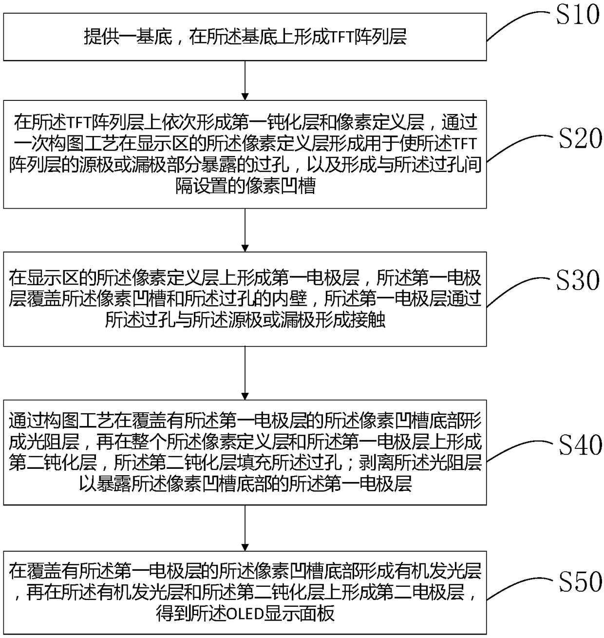
The embodiment of the invention provides a preparation method of an OLED display panel, comprising the following steps: providing a substrate, forming a TFT array layer, a first passivation layer anda pixel definition layer on the substrate; At least one via hole and at least one pixel groove are for on that pixel definition layer by a patterning process; Each of the vias is spaced apart from each of the pixel grooves; At least one first electrode lay is formed by continue preparation, that first electrode layer simultaneously covering the entire inner wall of the pixel groove and the via hole; Forming a photoresist layer on the first electrode layer on the bottom of the pixel groove, and forming a second passivation layer on the entire panel; Stripping the photoresist layer to expose thefirst electrode layer on the bottom of the pixel groove; An organic light emitting layer and a second electrode layer are formed on the first electrode layer on the bottom of the pixel groove to obtain the OLED display panel. The preparation method has the advantages of simple process and effective reduction of lateral light leakage phenomenon.

Description

technical field [0001] The invention relates to the field of display technology, in particular to a method for preparing an OLED display panel, an OLED display panel, and a display device. Background technique [0002] OLED (Organic Light-Emitting Diode, organic light-emitting diode), especially AMOLED (Active-matrix organic light emitting diode, active-matrix organic light-emitting diode) display technology has the advantages of wide color gamut, self-illumination, thinness and fast response speed. As the OLED display panel is more and more widely used, people's requirements for the display picture effect of the OLED display panel are also constantly increasing. [0003] In the production process of existing OLED display panels, colored organic photoresist materials are usually used as the pixel definition layer (PDL). However, these colored organic photoresist materials have high transmittance to visible light, which will lead to color saturation. The temperature drops, a...

Claims


Application Information

Patent Timeline
Patent Type & Authority Applications(China)
IPC IPC(8): H01L27/32H01L51/52H01L51/56
CPCH10K59/122H10K50/80H10K71/00
Inventor 周星宇
Owner TCL CHINA STAR OPTOELECTRONICS TECH CO LTD
Learn More