Graphene strip heterojunction double-gate tfet and its switching characteristic improvement method

A graphene and heterojunction technology, applied in semiconductor devices, electrical components, transistors, etc., can solve the problem of small on-state current, reduce leakage current, improve switching characteristics, and increase on-state current.

Active Publication Date: 2021-06-01
HANGZHOU DIANZI UNIV
View PDF6 Cites 0 Cited by
  • Summary
  • Abstract
  • Description
  • Claims
  • Application Information

AI Technical Summary

Problems solved by technology

[0004] The purpose of the present invention is to provide a graphene strip heterojunction double-gate TFET for the problem of small open-state current of the existing TFET device, and to provide a method for improving the switching characteristics of the double-gate TFET by using the graphene strip heterojunction method, this method utilizes the high electron mobility of graphene strips (GNR), and the bandgap size is regulated by the strip width and edge shape. GNRs with different edge shapes are used to form a heterojunction structure as the conductive channel of TFET. By adjusting the heterojunction shape and edge structure to control the quantum tunneling effect of electrons in the channel, it can improve the electrical performance of TFET

Method used


Image

  • Graphene strip heterojunction double-gate tfet and its switching characteristic improvement method
  • Graphene strip heterojunction double-gate tfet and its switching characteristic improvement method
  • Graphene strip heterojunction double-gate tfet and its switching characteristic improvement method

Examples


Embodiment Construction

[0019] The present invention will be further described below in conjunction with accompanying drawing.

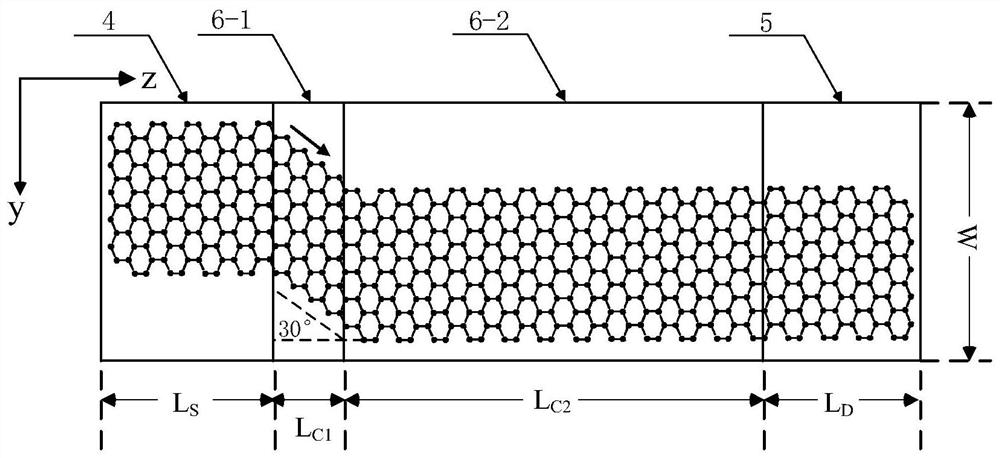
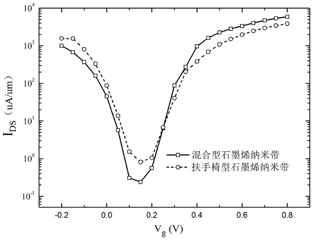
[0020] The present invention takes the double-gate TFET structure as an example, adopts figure 1 The hybrid graphene strips shown, demonstrate that this device structure can enhance the switching characteristics of TFETs.

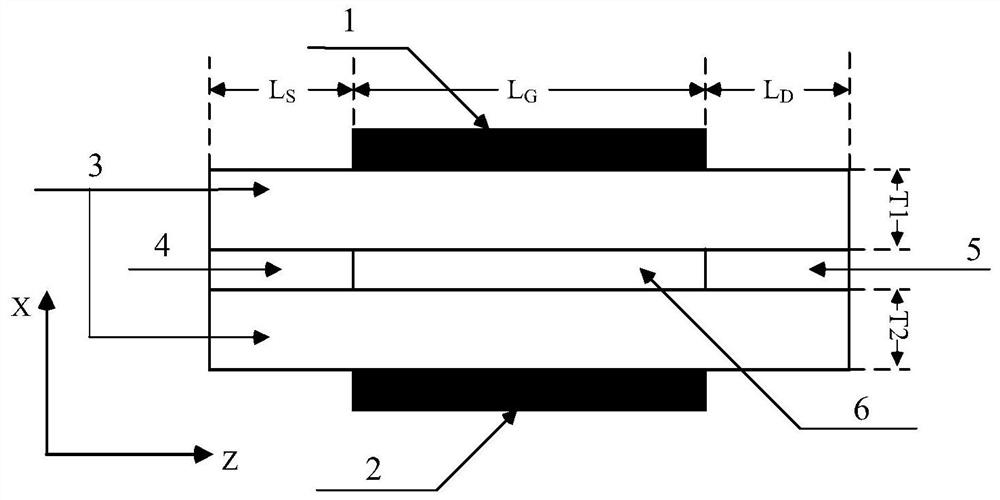
[0021] Such as figure 2 As shown, the graphene strip heterojunction double-gate tunneling field effect transistor (TFET) includes a top gate 1, a bottom gate 2, a gate oxide layer 3, a source region 4, a drain region 5 and a channel 6, wherein the gate The oxide layer is made of SiO 2 Materials; source region 4, drain region 5 and channel 6 are located between the top gate oxide layer 3 and the bottom gate oxide layer 3; the bottom gate 2 is located under the gate oxide layer 3 at the bottom, and the top gate 1 is located at the top gate oxide layer 3 above, and the top gate 1 and the bottom gate 2 are aligned with the channel 6 in the length directi...


PUM

PropertyMeasurementUnit
angleaaaaaaaaaa

Abstract

The invention discloses a graphene strip heterojunction double-gate TFET and a method for improving switching characteristics thereof. How to improve the on-state current of TFET is an important direction of TFET research. The source region, the drain region and the channel between the source region and the drain region of the present invention form a graphene strip heterojunction; the channel is composed of a first channel section and a second channel section arranged along the direction from the source region to the drain region ; The source region, the second section of the channel and the drain area are all armchair graphene nano-strips; the extending direction of the strips of the first channel and the extending direction of the armchair graphene nano-strips form an included angle. In the off state of the present invention, a section of the channel is a bandgap armchair graphene nano-strip along the length direction of the device, and the regional density of states is 0, which plays a role in suppressing the off-state current; in the on state, there is Current, one section of the channel is a zigzag graphene strip along the direction of current transmission, and there is no band gap in one section of the channel, which promotes the quantum tunneling effect of electrons between the source region and the channel, and increases the on-state current.

Description

technical field [0001] The invention belongs to the technical field of field effect transistors, and proposes a method for using a graphene heterojunction as a conductive channel of a tunneling field effect transistor (TFET) to improve the switching characteristics of the TFET. Background technique [0002] Since the invention of the IC, the Metal Oxide Field Effect Transistor (MOSFET) has been the most popular semiconductor device in the IC, and the feature size of the device has been shrinking according to the prediction of Moore's Law. With the continuous development of device miniaturization, a series of negative effects such as the "short channel effect" of MOSFET due to the shortened channel length have seriously affected the performance of MOSFET devices; The limitation of channel current and working principle leads to the fact that the sub-threshold swing of the MOSFET device cannot be lower than 60meV / dec, and the power consumption of the device is large, which also...

Claims


Application Information

Patent Timeline
Patent Type & Authority Patents(China)
IPC IPC(8): H01L29/739H01L29/10H01L29/06H01L29/165H01L21/331
CPCH01L29/0665H01L29/1029H01L29/1606H01L29/165H01L29/66045H01L29/7391
Inventor 王晶封路阮良浩赵文生张海鹏
Owner HANGZHOU DIANZI UNIV
Why Eureka
Try Eureka