Radio frequency probe for testing PCB board impedance

A PCB board and radio frequency technology, applied in the field of radio frequency probes, can solve problems such as PCB board impedance testing, achieve the effects of good contact, simple processing, and avoid damage to the needle

Pending Publication Date: 2018-12-21
上海军友射频技术有限公司
View PDF0 Cites 3 Cited by
  • Summary
  • Abstract
  • Description
  • Claims
  • Application Information

AI Technical Summary

Problems solved by technology

[0005] The object of the present invention is to overcome the above-mentioned deficiencies, provide a kind of electrical and radio frequency stable test PCB board impedance radio frequency probe, realize the reliable and stable test of PCB board by radio frequency probe within the specified frequency range, solve the problem of PCB board impedance test

Method used


Image

  • Radio frequency probe for testing PCB board impedance
  • Radio frequency probe for testing PCB board impedance
  • Radio frequency probe for testing PCB board impedance

Examples


Embodiment Construction

[0033] The present invention will be described in further detail below with reference to the accompanying drawings and specific embodiments, but it is not intended to limit the present invention.

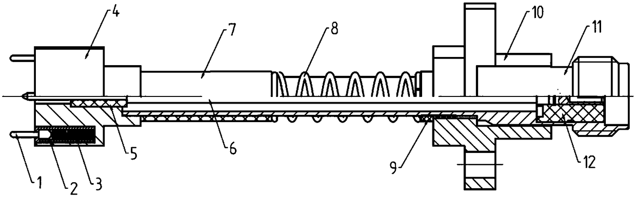
[0034] like Figure 3a and Figure 3b As shown, the RF probe for testing PCB board impedance of the present invention includes a grounding pin 1, a grounding shell 2, a grounding spring 3, a front-end outer conductor 4, a front-end insulator 5, a signal pin 6, an outer insulator 7, an outer conductor spring 8, a middle Insulator 9 , flange 10 , main outer conductor 11 , rear insulator 12 .

[0035] The front end insulator 5 is embedded in the front end outer conductor 4, and after the outer insulator 7 and the outer conductor spring 8 are sheathed outside the main outer conductor 11, the front end of the main outer conductor 11 is embedded in the inner hole of the front end outer conductor 4 and has an interference fit with the front end outer conductor 4; The insulator 7 is locat...


PUM


Abstract

The invention discloses a radio frequency (RF) probe for testing PCB board impedance. The RF probe comprises ground pins, a ground shell, a ground spring, a signal pin, and a flange; two ground pins and one signal pin are arranged; since the flange covers a main outer conductor shell in the testing process, three contact pins without eccentricity is guaranteed when the flange is pressed; three contact pins perfectly contact a testing point of a PCB board, the contact is good and non-eccentric; the RF probe joint type is a SMA female structure and adopts a standard structure; the RF probe is mature and stable, high in frequency and simple in processing; the probe use frequency is greater than the actual use frequency of the PCB board, the working frequency can completely adapt to the testing width required by the PCB board.

Description

technical field [0001] The invention relates to the technical field of radio frequency probes, in particular to a radio frequency probe for testing PCB board impedance. Background technique [0002] There will be various signal transmissions in the conductors in the PCB circuit board. When the frequency must be increased in order to increase its transmission rate, if the circuit itself is different due to factors such as etching, stack thickness, and wire width, it will cause changes in impedance value. Distorting its signal will cause the performance of the circuit board to decrease, so it is necessary to control the impedance value within a certain range. [0003] At this stage, the best way to test the impedance of the PCB board is to use the RF probe contact method. The signal with the actual impedance of the PCB board is transmitted to the testing instrument through the RF probe. like figure 1 and figure 2 As shown in the figure, because the distance (L) between th...

Claims


Application Information

Patent Timeline
Patent Type & Authority Applications(China)
IPC IPC(8): G01R1/067G01R27/02
CPCG01R1/067G01R27/02
Inventor 王明明杜怀亮余际园熊东
Owner 上海军友射频技术有限公司
Why Eureka
Try Eureka