SRAM memory cell
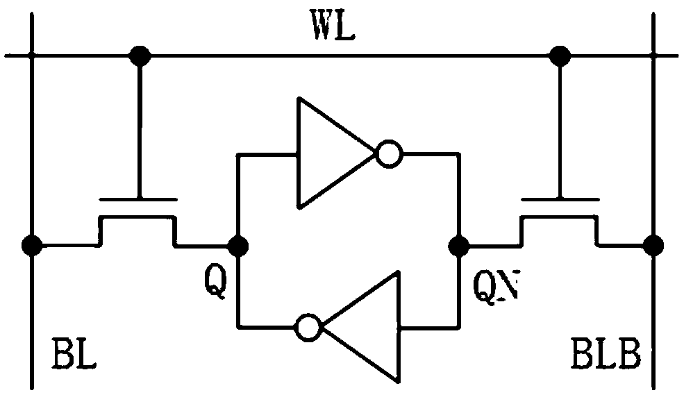
A storage unit and latch technology, used in information storage, static memory, read-only memory, etc., can solve the problems of lack of anti-softening, SRAM storage cells cannot be read and written, errors, etc., to achieve low read data time, Effects of high read static noise tolerance
- Summary
- Abstract
- Description
- Claims
- Application Information
AI Technical Summary
Problems solved by technology
Method used
Image
Examples
Embodiment Construction
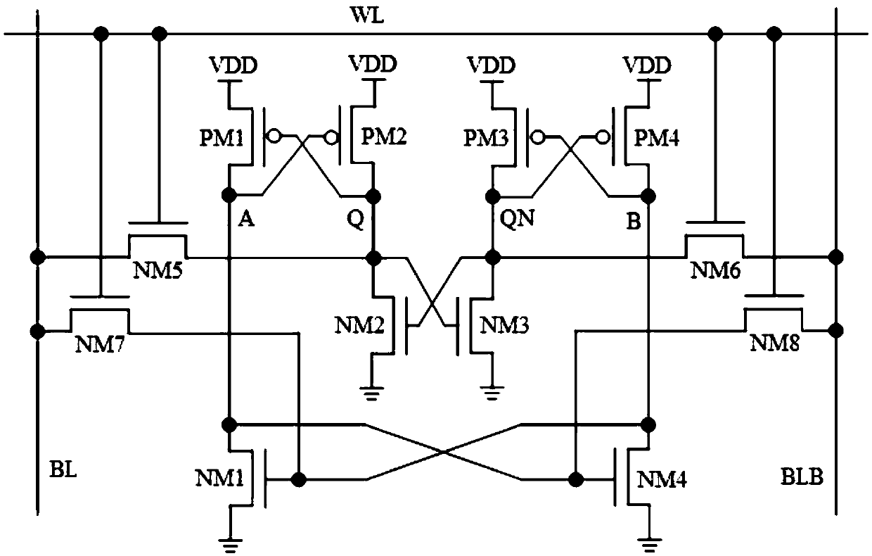
[0022] combine figure 1 As shown, in the following embodiments, the SRAM storage unit is composed of two sets of P-type cross-coupled latch structures, two sets of N-type cross-coupled latch structures, and four N-type transmission transistors, forming a possible The 12-transistor soft-error-resistant SRAM memory cell that works near the threshold voltage has the function of fast reading and writing.
[0023] The source of the PMOS transistor PM1 and the source of the PMOS transistor PM2 are connected to the power supply voltage terminal VDD, the gate of the PMOS transistor PM1 is connected to the drain of the PMOS transistor PM2, and the connected node is marked as Q, and the gate of the PMOS transistor PM2 The pole is connected to the drain of the PMOS transistor PM1, and the node connected thereto is denoted as A, forming a first group of P-type cross-coupled latch structures.
[0024] The source of the PMOS transistor PM3 and the source of the PMOS transistor PM4 are conn...
PUM
 Abstract
Description
Claims
Application Information


