

A negative group delay circuit based on RLC and a low noise amplifier and a design method thereof
A low-noise amplifier and negative group delay technology, which is applied to electrical components, impedance networks, multi-terminal pair networks, etc.
- Summary
- Abstract
- Description
- Claims
- Application Information
AI Technical Summary
Problems solved by technology
Method used
Image

Examples
Embodiment Construction
[0062] The present invention is described in further detail now in conjunction with accompanying drawing.
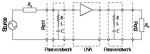
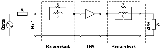
[0063] Such as figure 1 Shown, a kind of negative group delay circuit based on serial RLC and low noise amplifier is characterized in that: comprise signal source, described signal source is connected with network input port, and described network input port is connected with network output port, The network output port is connected to an external load, and the impedance of the signal source and the load impedance are both R 0 , two groups of RLC-based resonant circuits are arranged between the network input port and the network output port, and a low-noise amplifier is connected between the two groups of RLC-based resonant circuits, and the RLC-based resonant circuit consists of resistors R, The inductance L and the capacitance C are sequentially connected in series, and the resonant circuit based on RLC is connected in parallel between the network input port and the n...
PUM
 Abstract
Description
Claims
Application Information