High-current carrying capacity multilayer ceramic substrate and manufacturing method thereof

A multi-layer ceramic and manufacturing method technology, which is applied in semiconductor/solid-state device manufacturing, electrical components, electrical solid-state devices, etc., can solve the problems of reduced wiring density and assembly density, affecting system miniaturization, etc., and achieves improvement of current carrying capacity Effect

Pending Publication Date: 2019-01-01
NO 43 INST OF CHINA ELECTRONICS TECH GRP CETC
View PDF0 Cites 0 Cited by
  • Summary
  • Abstract
  • Description
  • Claims
  • Application Information

AI Technical Summary

Problems solved by technology

If the circuit substrate wiring passes a large current, the conductor wiring must be widened, but widening the conductor wiring will reduce the wiring density and assembly density, which will affect the original intention of the miniaturization of the system
Therefore, the existing multilayer ceramic substrate is only suitable for circuit products with low power, and it is not suitable for circuit products with high power, such as power modules, planar transformers with high power, and wiring substrates with large currents. Film Multilayer Wiring Conductor

Method used


Image

  • High-current carrying capacity multilayer ceramic substrate and manufacturing method thereof
  • High-current carrying capacity multilayer ceramic substrate and manufacturing method thereof
  • High-current carrying capacity multilayer ceramic substrate and manufacturing method thereof

Examples


Embodiment 1

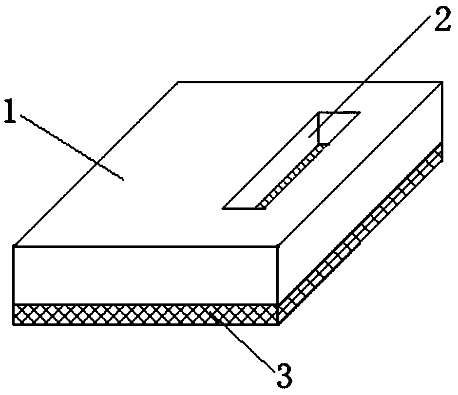
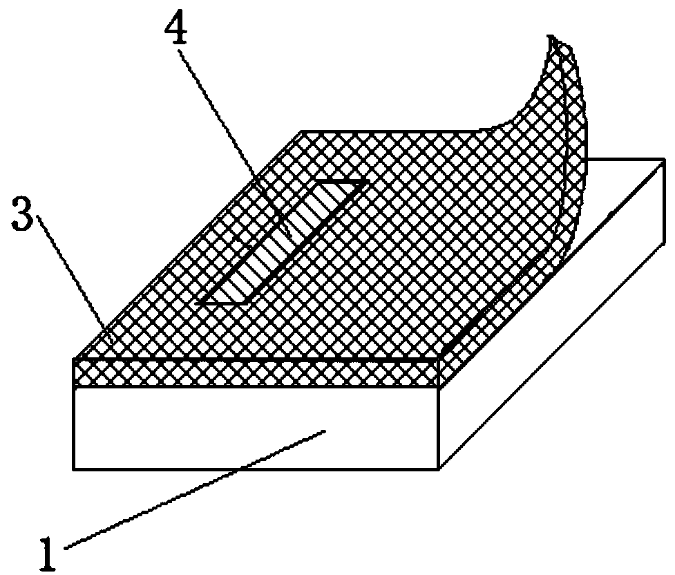
[0043] Embodiment 1: LTCC (low temperature co-fired ceramic) ceramic tape is used to make a substrate of straight wire with high current-carrying capacity. In this embodiment, the wiring length of the straight wire is ≤10 mm. The tape-cast green ceramic sheet 1 is formed by using a square punch with a side length of 0.3mm through one continuous punch figure 2 For the shown continuous through groove 2, in this embodiment, the green ceramic sheet 1 is covered with a back film 3, and the leakage position of the back film 3 is the same as that of the continuous through groove 2, and then the groove is filled with a conductive paste 4, baked After drying, remove the backing film 3 as image 3 As shown, the green ceramic sheet 1 filled with conductive paste 4 is obtained, such as Figure 4 As shown, electrodes and wires are printed on the green ceramic sheet 1. After the conductor is dried, take the three-layer green ceramic sheets L1, L2, and L3 and carry out alignment laminati...

Embodiment 2

[0044] Embodiment 2: A substrate of a square spiral wire with high current-carrying capacity is manufactured by using LTCC green ceramic tape. The tape-cast green ceramic sheet is punched twice with a circular punch with a diameter of 0.1 mm to form a continuous square spiral through groove. In this embodiment, the stepping distance of the circular punch is selected as circular punch. 1 / 2 of the head diameter (relative to edge flatness H / D = 86.6%). Perform the first segmental punching to form several spaced through grooves on the green ceramic sheet, and fill the grooves with conductive paste, such as Figure 6 As shown, after drying, the second segmental slotting is performed at the interval between adjacent through-slots formed by the first segmental slotting, and then the slots are filled with conductive paste and dried to form an overall continuous square spiral through-slot ,Such as Figure 7 As shown, then print electrodes and wires, etc. After drying, each layer of ...

Embodiment 3

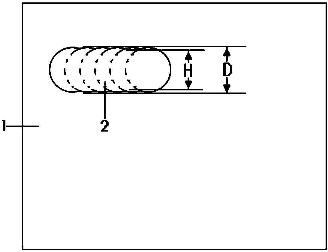
[0045] Embodiment 3: A substrate of a circular spiral wire with high current-carrying capacity is manufactured by using LTCC green ceramic tape. The tape-cast green ceramic sheet is formed with a circular punch with a diameter of 0.4 mm to form a continuous circular spiral through groove through two segmental punches. In this embodiment, the stepping distance of the circular punch is selected as circular. 1 / 4 of the diameter of the punch (relative to the edge flatness H / D=96.8%), perform the first segmental punching to form several spaced through grooves on the green ceramic sheet, fill the grooves with conductive paste, and after drying, Carry out the second segmental punching at the interval between adjacent through-slots formed by the first segmental punching, and then fill the slots with conductive paste and dry to form an overall continuous circular spiral through-slot, such as Figure 8 As shown, then print electrodes and wires, etc. After drying, each layer of green ce...


PUM

PropertyMeasurementUnit
thicknessaaaaaaaaaa

Abstract

The invention discloses a high-current carrying capacity multilayer ceramic substrate and a manufacturing method thereof. According to the high-current carrying capacity multilayer ceramic substrate and the manufacturing method thereof of the invention, a continuous through groove is formed in a green tape by means of continuous punching; the continuous through groove is filled with conductors, sothat the conductors can be arranged; and therefore, the wiring thickness of the conductors can be greatly increased, and the current-carrying capacity of the multilayer ceramic substrate is significantly enhanced, more large-power circuit products can be miniaturized, planarized, and integrated by using the multilayer wired ceramic substrate, and the integration of such circuit products can be improved.

Description

technical field [0001] The invention relates to the field of electronic devices, in particular to a multilayer ceramic substrate with high current-carrying capacity and a manufacturing method thereof. Background technique [0002] The multilayer ceramic substrate can miniaturize and integrate the electronic equipment system, and the current carrying capacity of the wiring conductor in the multilayer ceramic substrate has a great influence on the reliability of the substrate. Existing multilayer ceramic substrates are formed by punching, filling, wiring, and then stacking, compacting and sintering multiple green ceramic sheets, while the wiring on the green ceramic sheets is usually formed by screen printing thick film process . When the screen printing thick film process is used, the thickness of the wiring is related to the printing screen of the screen printing (involving the screen wire diameter, mesh number, latex thickness, etc.), printing parameters (involving the har...

Claims


Application Information

Patent Timeline
Patent Type & Authority Applications(China)
IPC IPC(8): H01L23/498H01L21/48
CPCH01L23/49822H01L23/49827H01L21/4857H01L21/486
Inventor 李建辉项玮马涛沐方清李峰王秀文
Owner NO 43 INST OF CHINA ELECTRONICS TECH GRP CETC
Why Eureka
Try Eureka