Image sensor and forming method thereof

An image sensor and amorphous carbon technology, which is applied in the direction of electric solid devices, semiconductor devices, electrical components, etc., can solve the problems of reducing the transmission speed and service life of image sensors, so as to improve service life, increase transmission speed, and high thermal conductivity Effect

Inactive Publication Date: 2019-01-04
HUAIAN IMAGING DEVICE MFGR CORP
View PDF4 Cites 4 Cited by
  • Summary
  • Abstract
  • Description
  • Claims
  • Application Information

AI Technical Summary

Problems solved by technology

[0004] However, the use of silicon nitride is easy to reduce the transmission speed and service life of the image sensor

Method used


Image

  • Image sensor and forming method thereof
  • Image sensor and forming method thereof
  • Image sensor and forming method thereof

Examples


Embodiment Construction

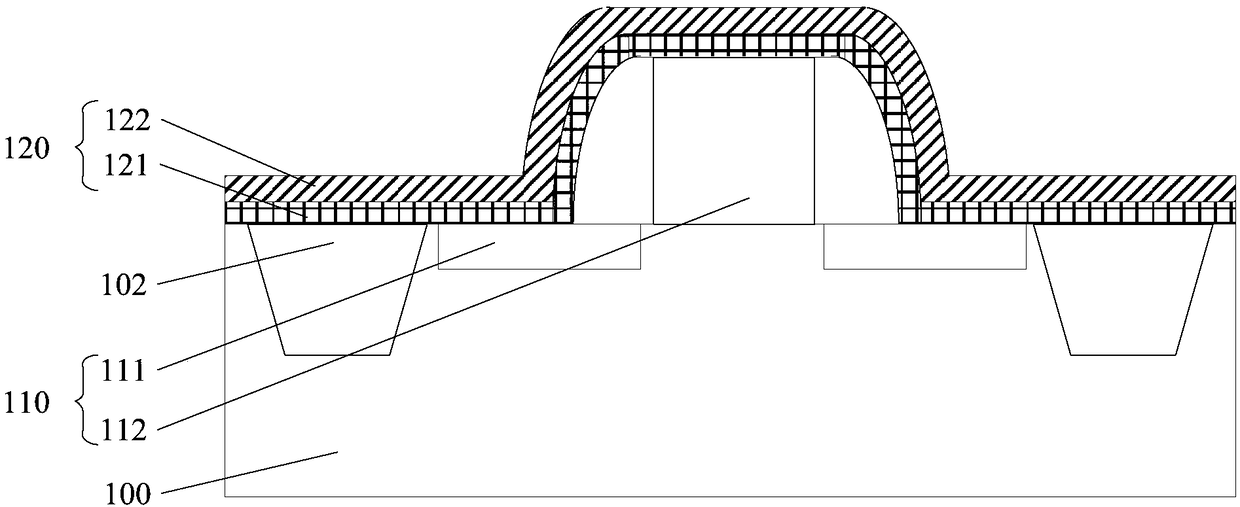
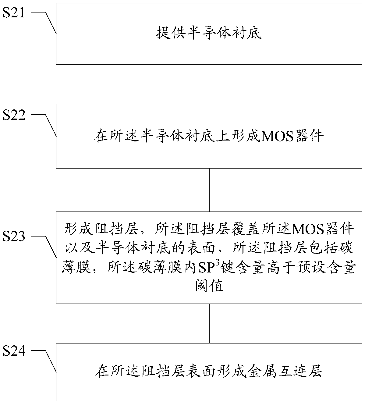
[0023] In the prior art, a semiconductor substrate is provided; a MOS device is formed on the semiconductor substrate; a barrier layer is formed, the barrier layer covers the surface of the MOS device and the semiconductor substrate, the barrier layer includes a carbon film, The carbon film within the SP 3 The bond content is higher than a preset content threshold; a metal interconnection layer is formed on the surface of the barrier layer. Using the above scheme, after forming MOS devices on the semiconductor substrate, silicon nitride and silicon dioxide are usually used as silicide barrier layers to protect the semiconductor substrate and MOS devices, so as to reduce the generation of metal interconnection layers in the subsequent formation. The effect, especially in the pixel area, can effectively reduce the generation of white points through protection.

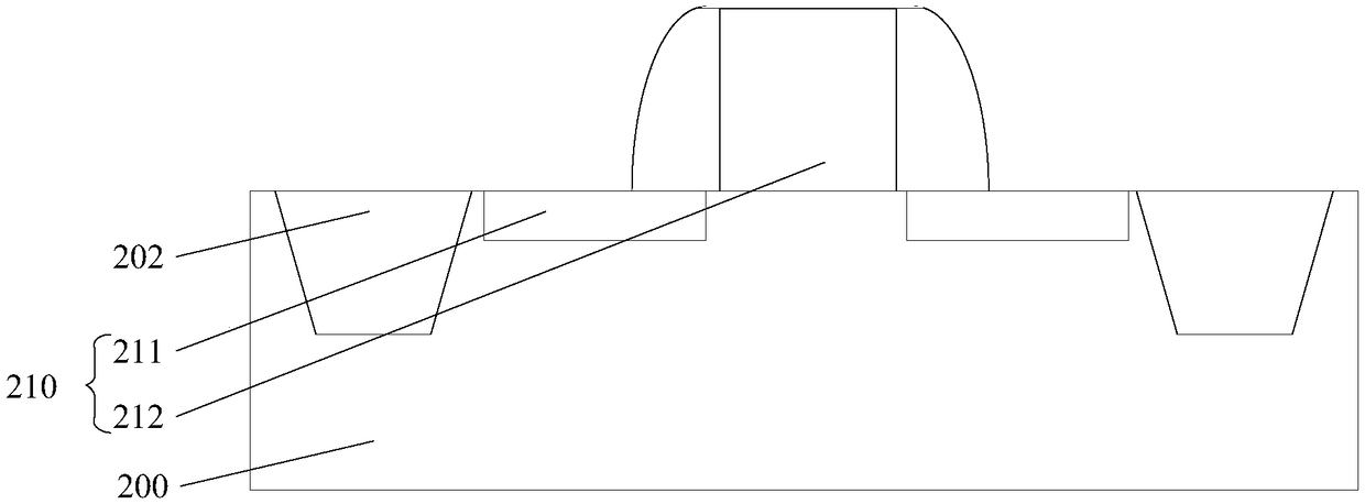
[0024] refer to figure 1 , figure 1 It is a schematic diagram of a device cross-sectional structure of an image sen...


PUM

PropertyMeasurementUnit
thicknessaaaaaaaaaa
thicknessaaaaaaaaaa

Abstract

An image sensor and a forming method thereof, the forming method comprising: providing a semiconductor substrate; Forming a MOS device on the semiconductor substrate; Forming a barrier layer coveringthe surface of the MOS device and the semiconductor substrate, wherein the barrier layer comprises a carbon film, and the SP3 bond content in the carbon film is higher than a preset content thresholdvalue; A metal interconnect lay is formed on that surface of the barrier layer. The scheme of the invention can improve the transmission speed and the service life of the image sensor.

Description

technical field [0001] The invention relates to the technical field of semiconductor manufacturing, in particular to an image sensor and a forming method thereof. Background technique [0002] The image sensor is the core component of the camera equipment, which realizes the image capture function by converting the optical signal into an electrical signal. Taking Complementary Metal Oxide Semiconductor Image Sensors (CMOS Image Sensors, CIS) devices as an example, due to their advantages of low power consumption and high signal-to-noise ratio, they have been widely used in various fields. [0003] In the prior art, after forming a Metal-Oxide-Semiconductor (MOS) device on a semiconductor substrate, silicon nitride (SiN or Si 3 N 4 ) and silicon dioxide (SiO 2 ) as a self-aligned silicide barrier layer (Self-Align Silicide Block or Salicide block, SAB), to protect the semiconductor substrate and MOS devices, so as to reduce the impact of the subsequent formation of metal i...

Claims


Application Information

Patent Timeline
Patent Type & Authority Applications(China)
IPC IPC(8): H01L27/146
CPCH01L27/1462H01L27/14636H01L27/14643
Inventor 鲁旭斋吴孝哲张锋吴龙江林宗贤
Owner HUAIAN IMAGING DEVICE MFGR CORP
Why Eureka
Try Eureka