An electroluminescence display panel and a display device
An electroluminescent display and panel technology, which is applied in the direction of circuits, electrical components, electric solid devices, etc., can solve problems that affect the service life of the light-emitting layer
- Summary
- Abstract
- Description
- Claims
- Application Information
AI Technical Summary
Problems solved by technology
Method used
Image
Examples
Embodiment
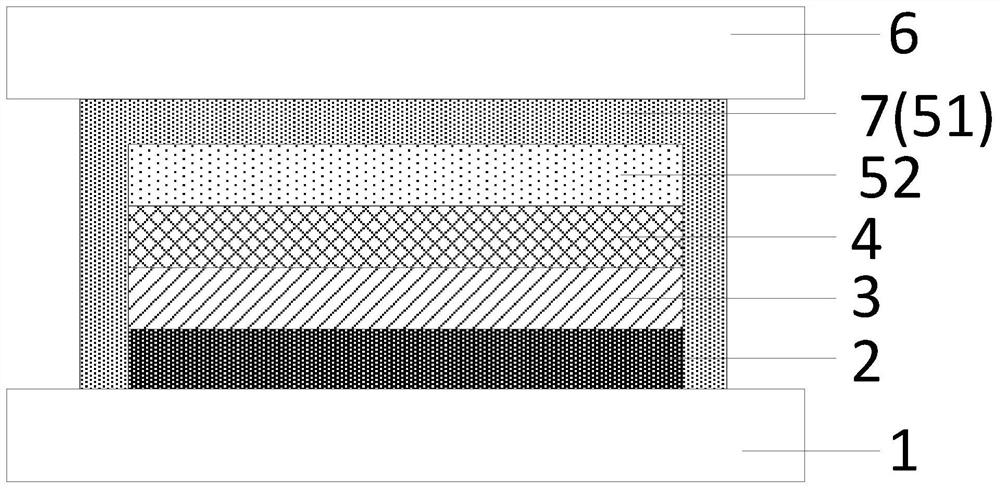
[0066] Such as Figure 4 As shown, when the encapsulation adhesive layer 7 is reused as the first conversion layer 51, one of Tb3+ / Yb3+ or Ce3+ / Yb3+ ion pairs is mixed in the encapsulation adhesive layer 7, and the ion exists in the form of nano-oxide co-doped particles ( Such as Tb3+ and Yb3+ co-doped YAG, Y2O3, TiO2 and other transparent nanoparticles) or organic small molecule complexes (organic small molecule complexes containing Tb3+ and Yb3+ ions at the same time), physically mixed into the adhesive material of the packaging adhesive layer 7 . The molar ratio of the sensitizer ion to the activator ion is selected between 1:1-1:5, and the doping weight percentage in the encapsulation adhesive layer 7 is between 1%-10%. These two ions, Tb3+ and Ce3+, have a good absorption effect on ultraviolet light with a wavelength in the range of 250nm to 350nm, and transfer energy to Yb3+ to convert it into near-infrared light at 900 to 1100nm.
[0067]When the oxide encapsulation l...
PUM
 Abstract
Description
Claims
Application Information


