Supercharge Your Innovation With Domain-Expert AI Agents!

High Dynamic Range Imaging Sensor Array

An imaging sensor and pixel sensor technology, applied in image communication, semiconductor devices, electric solid-state devices, etc., can solve the problem of limiting the degree of imaging in low-light areas

Active Publication Date: 2021-04-23
BAE SYST IMAGING SOLUTIONS
View PDF9 Cites 0 Cited by
  • Summary
  • Abstract
  • Description
  • Claims
  • Application Information

AI Technical Summary

Problems solved by technology

[0005] While providing a second photodiode in each pixel sensor extends the high-intensity response of the pixel sensor, various noise sources limit how well low-light areas can be imaged with reasonable exposure times

Method used


Image

  • High Dynamic Range Imaging Sensor Array
  • High Dynamic Range Imaging Sensor Array
  • High Dynamic Range Imaging Sensor Array

Examples


Embodiment Construction

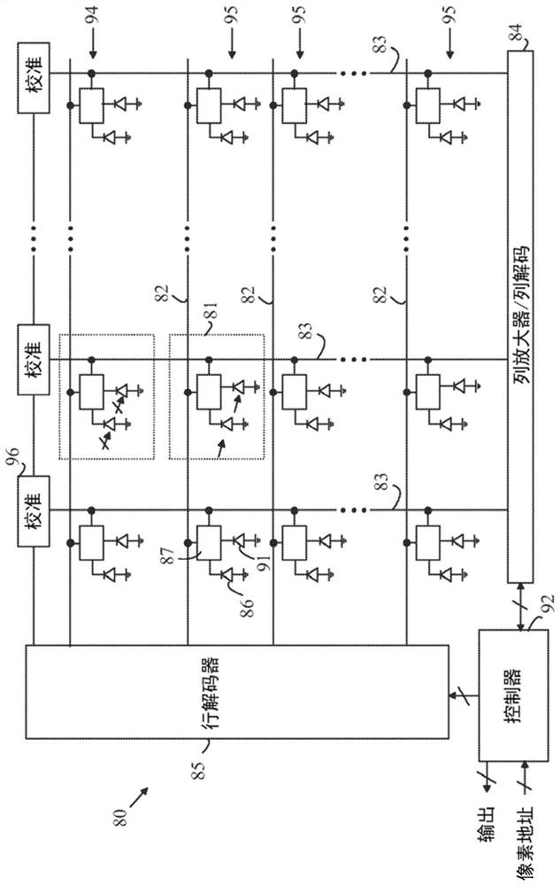
[0018] To simplify the following discussion, a pixel sensor is defined as a circuit that converts light incident on it into an electrical signal whose magnitude is determined by the amount of light incident on the circuit over a period of time, called exposure. The pixel sensor has a gate that is responsive to a signal on a row select line to couple the electrical signal to a readout line.

[0019] A rectangular imaging array is defined as a plurality of pixel sensors organized into rows and columns of pixel sensors. The rectangular array includes a plurality of readout lines and a plurality of row select lines, each pixel sensor is connected to a row select line and a readout line, the electrical signal generated by the pixel is responsive to the row select line associated with the pixel sensor The signal on , is connected to the readout line associated with that pixel.

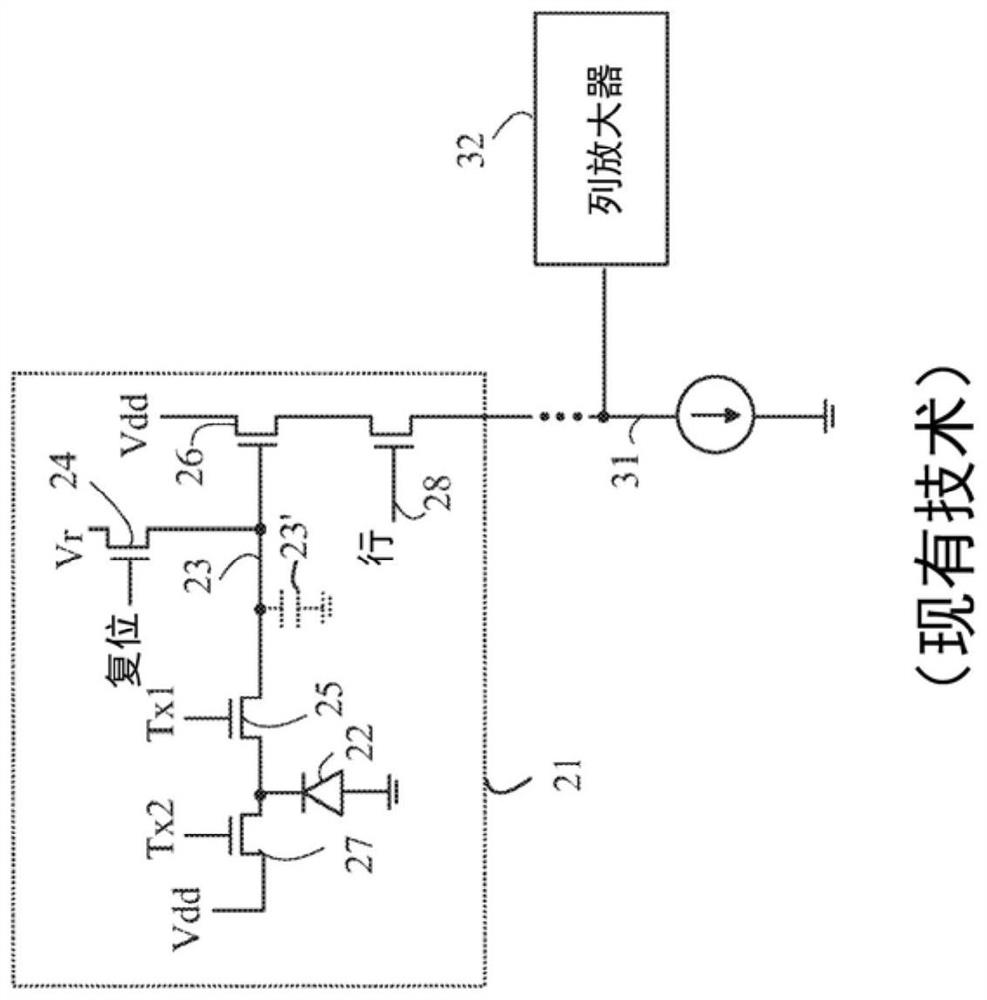
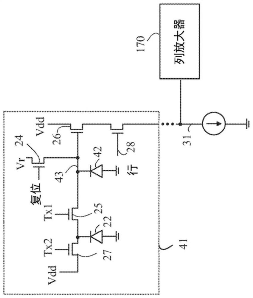
[0020] refer to figure 1 , the manner in which the present invention provides its advantages can be mor...


PUM


Abstract

The present invention discloses a device with a rectangular imaging array, characterized by a plurality of pixel sensors and a plurality of readout lines. The device has a plurality of column processing circuits, each column processing circuit connected to a corresponding one of the readout lines and a plurality of signal injectors, one signal injector connected to each readout line. Each signal injector couples one of a predetermined number of voltages to the sense line. The exposure of each pixel sensor is determined during an image recording cycle. The signal injector injects a plurality of calibration voltages into the readout lines and determines a gain function of amplifiers in a column processing circuit by measuring the outputs of the amplifiers for the plurality of calibration voltages during calibration periods between imaging recording periods.

Description

technical field [0001] The present invention relates to high dynamic range imaging sensor arrays. Background technique [0002] CMOS cameras typically form an image of a scene by imaging light from the scene onto an array of pixel sensors. Typically, each pixel sensor has one or more photodetectors. Each photodetector converts light received during exposure into an electrical signal. The electrical signal is then digitized by an analog-to-digital converter (ADC) to produce a digital value representing the amount of light received during the exposure period. The array is typically a two-dimensional array of pixels with thousands of columns and rows. The array is read out one row at a time using a separate column amplifier and ADC for each row. [0003] Typically, photodiodes have some range where the signal from the photodiode is a monotonically increasing function of the light received during the exposure period. At the bottom of the range, the accuracy of determining l...

Claims


Application Information

Patent Timeline
Patent Type & Authority Patents(China)
IPC IPC(8): H04N5/353H04N5/355H04N5/341H04N5/361H04N23/12
CPCH04N25/58H04N25/585H04N25/671H04N25/677H04N25/766H04N25/63H04N25/78H04N25/51H01L27/14609H04N25/75H04N25/40H04N25/67H04N25/581
Inventor B·穆A·M·麦格纳尼S·W·米姆斯
Owner BAE SYST IMAGING SOLUTIONS
Features
  • R&D
  • Intellectual Property
  • Life Sciences
  • Materials
  • Tech Scout
  • Unparalleled Data Quality
  • Higher Quality Content
  • 60% Fewer Hallucinations
Learn More