Controller, manufacturing method thereof, and monitoring method for chemical mechanical abrasive defects

A technology of chemical machinery and manufacturing methods, applied in semiconductor/solid-state device manufacturing, semiconductor/solid-state device testing/measurement, electrical components, etc., can solve problems such as low contrast, low capture rate, and increased wafer defect rate problem, to achieve the effect of improving contrast and crawling rate

Active Publication Date: 2019-01-08
SHANGHAI HUALI MICROELECTRONICS CORP
View PDF5 Cites 2 Cited by
  • Summary
  • Abstract
  • Description
  • Claims
  • Application Information

AI Technical Summary

Problems solved by technology

However, because the initial surface of the control sheet is a flat plane, when the defects formed are relatively shallow, the contrast between these defects and the background on the surface of the control sheet after chemical mechanical polishing will not be high, which will lead to The capture rate of these defects by the optical scanning machine is low (that is, missed detection occurs), which affects the accuracy of defect monitoring in the chemical mechanical polishing process, which in turn leads to an increase in the defective rate of subsequent processed wafers

Method used


Image

  • Controller, manufacturing method thereof, and monitoring method for chemical mechanical abrasive defects
  • Controller, manufacturing method thereof, and monitoring method for chemical mechanical abrasive defects
  • Controller, manufacturing method thereof, and monitoring method for chemical mechanical abrasive defects

Examples


Embodiment Construction

[0045] In order to make the purpose, advantages and characteristics of the present invention clearer, the following in conjunction with the attached Figure 1-7The control sheet proposed by the present invention, its manufacturing method and the monitoring method of chemical mechanical polishing defects are further described in detail. It should be noted that all the drawings are in a very simplified form and use imprecise scales, and are only used to facilitate and clearly assist the purpose of illustrating the embodiments of the present invention.

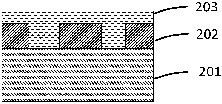
[0046] An embodiment of the present invention provides a control sheet, refer to Figure 2a , Figure 2a It is a schematic longitudinal cross-sectional view of a control sheet according to an embodiment of the present invention, and the control sheet includes: a substrate 201 , a patterned first dielectric layer 202 and a second dielectric layer 203 . Wherein, the patterned first dielectric layer 202 is formed on the upper surf...


PUM

PropertyMeasurementUnit
thicknessaaaaaaaaaa
thicknessaaaaaaaaaa

Abstract

A control sheet is manufactured by forming a patterned first dielectric layer on an upper surface of a substrate and a second dielectric layer that fills grooves of at least the patterned first dielectric layer, and a method of manufacturing the control sheet and a method of monitoring chemical-mechanical polishing defects. The control sheet is placed on a chemical mechanical grinding machine andground for treatment to remove the first dielectric layer; Then, the surface of the treated control sheet is scanned to obtain defects of the upper surface of the control sheet to achieve monitoring of the chemical mechanical grinding defects. The control sheet provided by the invention improves the comparison degree between the defects on the surface of the control sheet and the background, further improves the grasping rate of the defects caused by the chemical mechanical polishing by the optical scanner table, and realizes the effective monitoring of the chemical mechanical polishing defects.

Description

technical field [0001] The invention relates to the technical field of semiconductor manufacturing, in particular to a control chip, a manufacturing method thereof, and a monitoring method for chemical mechanical polishing defects. Background technique [0002] In the manufacturing process of semiconductor wafers, a chemical mechanical polishing (CMP) process plays an important role in flattening the surface of the wafer. However, in the chemical mechanical polishing process, the particles in the polishing liquid and the damaged polishing pad will cause defects such as scratches and pits on the surface of the product, and when the size of the particles in the polishing liquid increases due to crystallization or the polishing pad is damaged due to When the damage is severe due to excessive use for a long time, the number of defects will increase, and the size will also increase, which will lead to a decrease in the yield of the wafer. Therefore, if the defects can be detecte...

Claims


Application Information

Patent Timeline
Patent Type & Authority Applications(China)
IPC IPC(8): H01L21/67H01L21/311H01L21/3105H01L21/306H01L21/66
CPCH01L21/30604H01L21/30625H01L21/31055H01L21/31111H01L21/67253H01L22/12
Inventor 袁增艺龙吟倪棋梁
Owner SHANGHAI HUALI MICROELECTRONICS CORP
Why Eureka
Try Eureka