Display substrate, method of manufacturing the same, and display device

A technology for display substrates and display devices, applied in the fields of final product manufacturing, sustainable manufacturing/processing, organic semiconductor devices, etc., can solve the problems of poor display brightness uniformity of display substrates, and achieve the effect of good display brightness uniformity

Active Publication Date: 2019-01-11
BOE TECH GRP CO LTD
View PDF3 Cites 1 Cited by
  • Summary
  • Abstract
  • Description
  • Claims
  • Application Information

AI Technical Summary

Problems solved by technology

[0005] Embodiments of the present invention provide a display substrate, a manufacturing method thereof, and a display device, which can solve the problem of poor display brightness uniformity of the display substrate in the related art

Method used


Image

  • Display substrate, method of manufacturing the same, and display device
  • Display substrate, method of manufacturing the same, and display device
  • Display substrate, method of manufacturing the same, and display device

Examples


Embodiment Construction

[0053] In order to make the object, technical solution and advantages of the present invention clearer, the implementation manner of the present invention will be further described in detail below in conjunction with the accompanying drawings.

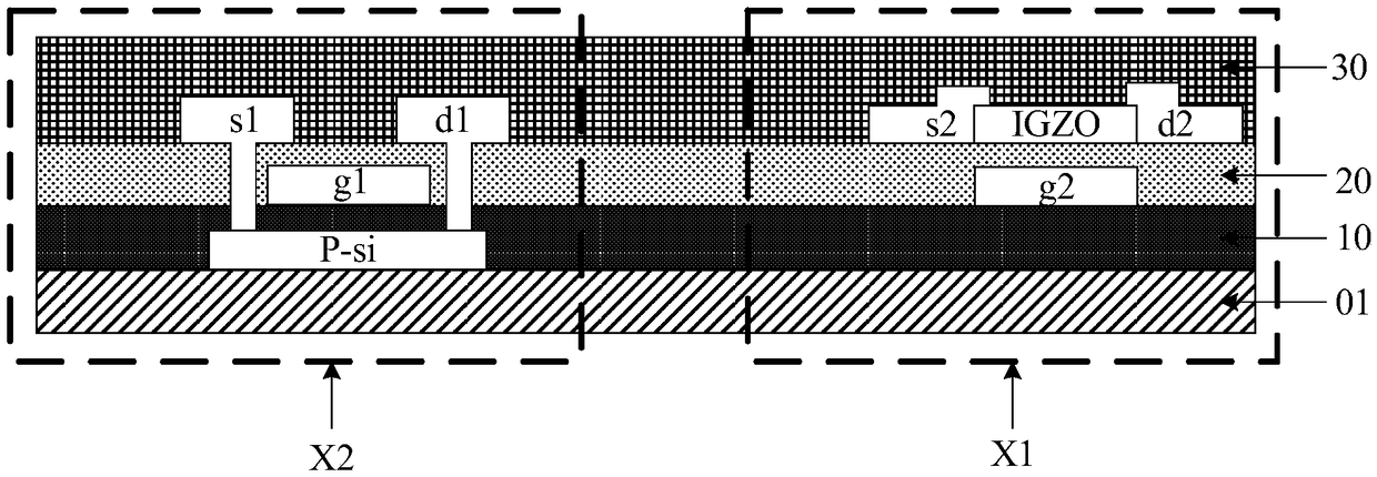
[0054] The display substrate provided in the embodiment of the present invention may be an LTPO display substrate. figure 1 It is a schematic structural diagram of an LTPO display substrate provided by an embodiment of the present invention, as shown in figure 1 As shown, the LTPO display substrate may include a pixel area X1 and a peripheral circuit area X2.

[0055] Wherein, the driving transistor disposed in the peripheral circuit area X2 may be an LTPS TFT, and the active layer of the LTPS TFT may be made of P-type silicon (P-si) material. refer to figure 1 It can be seen that the active layer of the LTPS TFT is disposed on the base substrate 01 , and a gate insulating layer 10 is disposed on the side of the active layer away fro...


PUM


Abstract

The invention discloses a display substrate and a manufacturing method thereof, and a display device and belongs to the technical field of display. The display substrate may include a plurality of pixel units disposed on a substrate; an encapsulation layer arranged on a side of the plurality of pixel units remote from the substrate; a conductive film layer disposed on a side of the encapsulation layer remote from the substrate; and a protective film layer arranged on a side of the conductive film layer remote from the substrate. Since the display substrate also includes a conductive film layerdisposed between the encapsulation layer and the protective film layer. When the protective film layer is torn, electrons generated by the electrostatic discharge phenomenon due to friction can be released to the conductive film layer. As that protective film layer is torn, the problem that electrons transition to the active layer of the transistor in the display substrate, thereby shifting the threshold voltage of the transistor is avoided. The display substrate provided by the invention has good uniformity of display brightness.

Description

technical field [0001] The invention relates to the field of display technology, in particular to a display substrate, a manufacturing method thereof, and a display device. Background technique [0002] Low Temperature Polycrystalline Oxide (LTPO) display substrate is a display substrate manufactured by using low temperature polycrystalline silicon (Low Temperature Polycrystalline, LTPS) thin film transistor (ThinFilm Transistor, TFT) and oxide (Oxide) TFT at the same time. [0003] In the related art, the LTPO display substrate includes: TFTs and active matrix organic light emitting diodes (Active Matrix Oxide Light Emitting Diode, AMOLED) formed on the LTPO backplane, which are sequentially stacked on the LTPO backplane formed with TFTs and AMOLEDs The encapsulation layer is a protective film layer formed on the side away from the encapsulation layer. [0004] However, before the signal wires in the display substrate are bound to the driving chip that drives the display s...

Claims


Application Information

Patent Timeline
Patent Type & Authority Applications(China)
IPC IPC(8): H01L27/32
CPCH10K59/12H10K59/1201Y02E10/549Y02P70/50H10K59/35H10K59/1213H10K71/80H10K77/111H10K50/8423H10K50/8445H10K2102/101H10K2102/341H10K2102/103H10K71/00H10K2102/351H10K2102/311
Inventor 刘文渠张锋姚琪吕志军董立文张世政党宁宋晓欣崔钊
Owner BOE TECH GRP CO LTD
Why Eureka
Try Eureka