Supercharge Your Innovation With Domain-Expert AI Agents!

Image sensor chip of a single-layer embedded biometrics algorithm and terminal device

An image sensor and biometrics technology, which is applied in the field of integrated circuit technology and biometrics, can solve problems that restrict the development of biometrics technology, and achieve the effects of promoting common development, low power consumption, and high security level

Pending Publication Date: 2019-01-15
深圳荆虹科技有限公司
View PDF9 Cites 0 Cited by
  • Summary
  • Abstract
  • Description
  • Claims
  • Application Information

AI Technical Summary

Problems solved by technology

[0004] Although iris recognition has begun to enter the intelligent terminal, there are two difficult problems that need to be solved in iris recognition: one is the acquisition of iris images, and the other is the realization of iris recognition. This is also the biggest bottleneck restricting the development of biometric technology, especially iris recognition. even more so with technology

Method used


Image

  • Image sensor chip of a single-layer embedded biometrics algorithm and terminal device
  • Image sensor chip of a single-layer embedded biometrics algorithm and terminal device
  • Image sensor chip of a single-layer embedded biometrics algorithm and terminal device

Examples


Embodiment Construction

[0031] In order to make the purpose, technical solutions and advantages of the embodiments of the present invention clearer, the technical solutions in the embodiments of the present invention will be clearly and completely described below in conjunction with the drawings in the embodiments of the present invention. Obviously, the described embodiments It is a part of embodiments of the present invention, but not all embodiments. Based on the embodiments of the present invention, all other embodiments obtained by persons of ordinary skill in the art without creative efforts fall within the protection scope of the present invention.

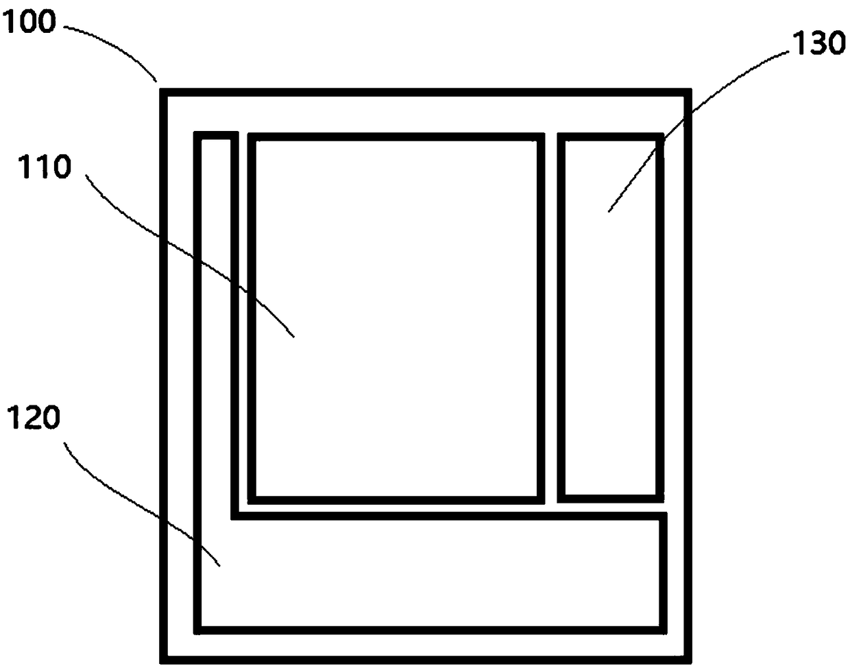
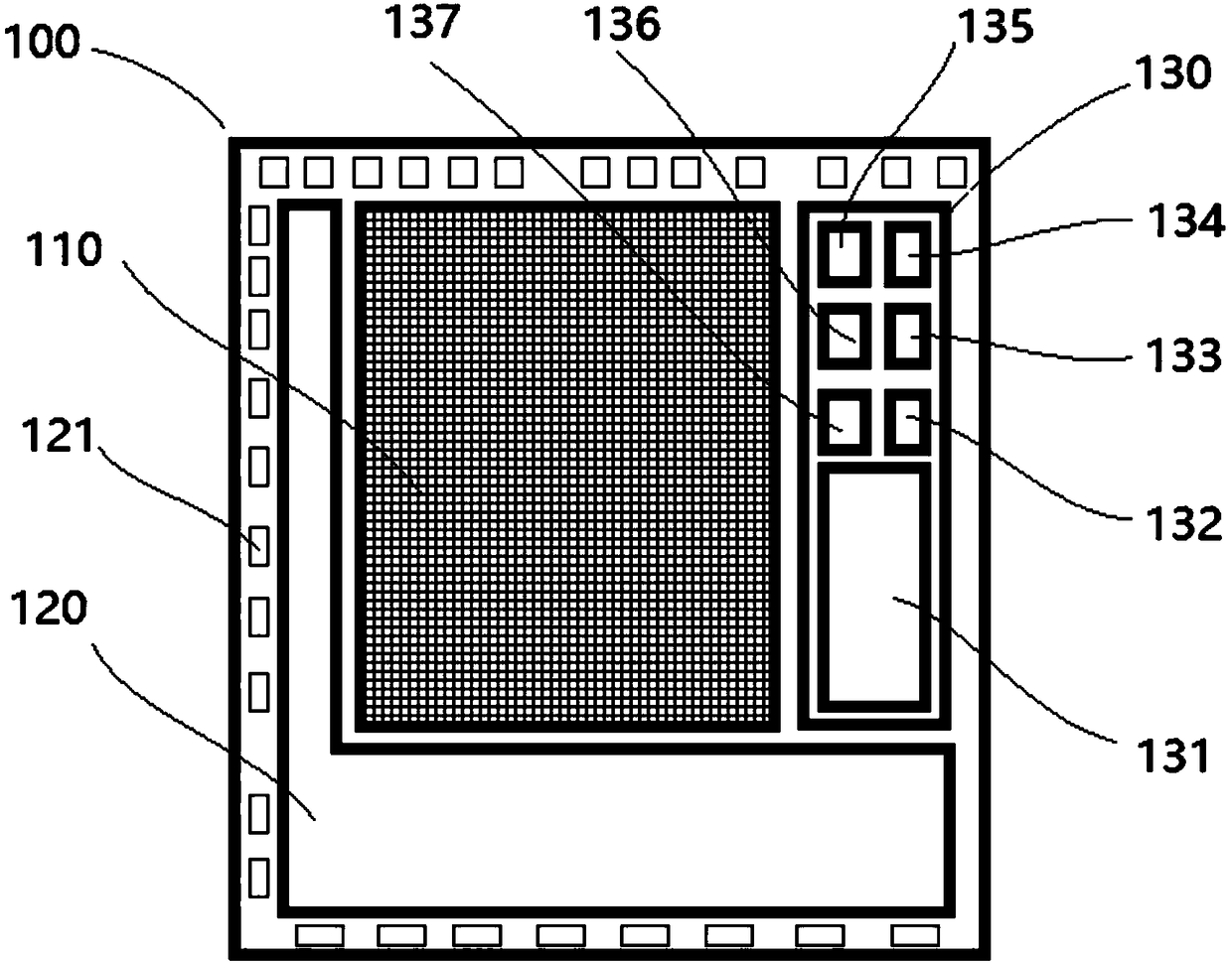
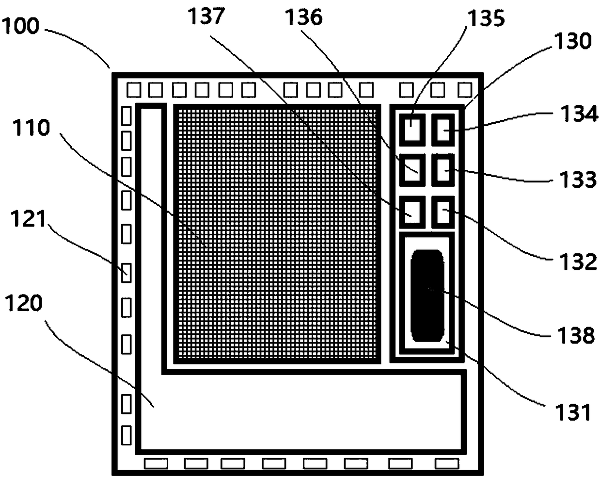
[0032] Figure 1 ~ Figure 3 A schematic structural diagram of an image sensor chip with a single-layer embedded biometric recognition algorithm provided by an embodiment of the present invention is shown. see Figure 1 ~ Figure 3 The image sensor chip 100 of a single-layer embedded biometric recognition algorithm provided by the embodiment of the ...


PUM


Abstract

The invention provides an image sensor chip of a single-layer embedded biometrics algorithm and a terminal device. The image sensor chip comprises a pixel module, a circuit module and a biometrics module which are arranged on the same medium layer and electrically connected. The pixel module is used to realize image acquisition and convert the collected optical signal into electrical signal. The circuit module is arranged on the periphery of the pixel module. The circuit module comprises an analog circuit part and a digital circuit part. At least a biometrics block is arranged in the biometrics module, a preset biometrics algorithm is arranged in the biometrics block, and the biometrics block is used for corresponding biometric identification of the digital signal outputted from the circuit module according to the preset biometrics algorithm built in the biometrics block. The image sensor chip provided by the invention can simultaneously realize biological image acquisition and biological identification functions, thereby making the function of the image sensor chip more powerful and the safety more improved.

Description

technical field [0001] The invention relates to the fields of integrated circuit technology and biometric identification technology, in particular to an image sensor chip and a terminal device with a single-layer embedded biometric identification algorithm. Background technique [0002] A major feature of the rapid development of informatization is the digitalization and invisibility of personal identities. How to accurately identify a person's identity and protect information security is a key social problem that must be solved in today's information age. With the rise of the Internet and smart terminals, people's awareness of security has gradually increased. Smart terminals not only automatically start items and some system permissions, but also involve unlocking, file system permissions, privacy and security, and secure payments. User management , thus deriving a series of security and confidentiality measures. [0003] Biometric identity authentication technology is a ...

Claims


Application Information

Patent Timeline
Patent Type & Authority Applications(China)
IPC IPC(8): G06K9/00
CPCG06V40/10G06V40/53G06V10/94G06V10/955
Inventor 黄欢赵刚
Owner 深圳荆虹科技有限公司
Features
  • R&D
  • Intellectual Property
  • Life Sciences
  • Materials
  • Tech Scout
  • Unparalleled Data Quality
  • Higher Quality Content
  • 60% Fewer Hallucinations
Learn More