

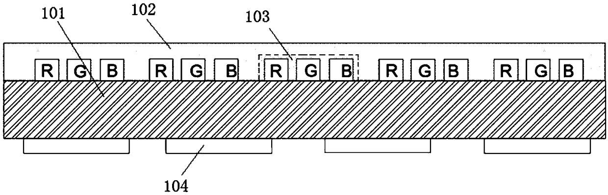
High-contrast COB packaged small-pitch LED display panel
A high-contrast, display panel technology, used in identification devices, instruments, electrical components, etc., can solve the problem that the brightness of LED light-emitting chips is not high, the contrast of small-pitch products cannot be larger, and the area of bonding pads cannot be very large. Small and other problems, to achieve the effect of reducing the design area of the pad, improving the brightness, and preventing the flow area from being too large
- Summary
- Abstract
- Description
- Claims
- Application Information
AI Technical Summary
Problems solved by technology
Method used
Image

Examples
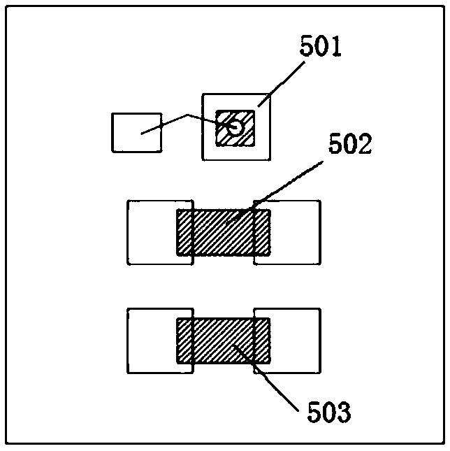
Embodiment 1
[0026] Such as Figure 2a As shown, the red LED light-emitting chip 501 adopts a vertical die-bonding structure, which requires wire bonding, while the green LED light-emitting chip 502 and blue LED light-emitting chip 503 adopt a flip-chip die-bonding structure, which does not require wire bonding, effectively saving pads Design area, reduce wire bonding area, improve contrast. The encapsulation adhesive layer 102 is blended with melanin with a total weight of 1‰ of the epoxy resin to further improve the contrast.
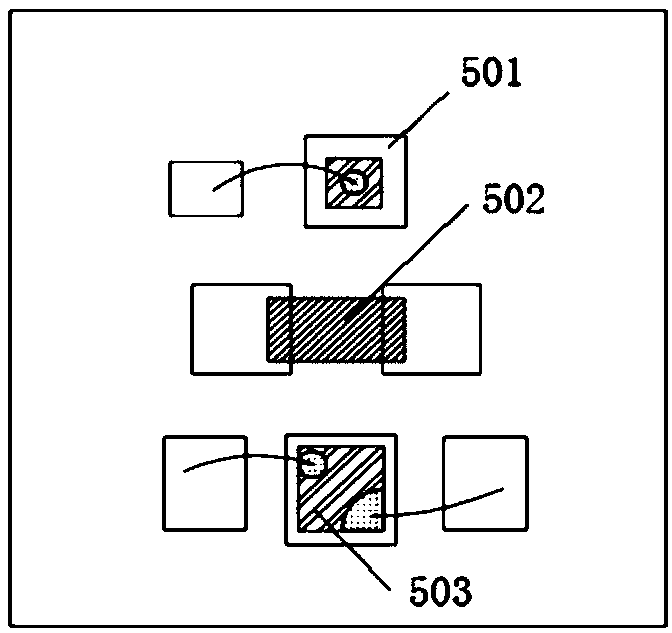
Embodiment 2
[0028] Such as Figure 2b As shown, the red LED light-emitting chip 501 and the blue LED light-emitting chip 503 adopt a vertical die-bonding structure, which requires wire bonding; the green LED light-emitting chip 502 adopts a flip-chip die-bonding structure, which does not require wire bonding, effectively saving pads Design area, reduce wire bonding area, improve contrast. The encapsulation adhesive layer 102 is blended with melanin with a total weight of 4‰ of the epoxy resin to further improve the contrast.
Embodiment 3
[0030] Such as Figure 2c As shown, the red LED light-emitting chip 501 and the green LED light-emitting chip 502 adopt a vertical die-bonding structure, which requires wire bonding; the blue LED light-emitting chip 503 adopts a flip-chip die-bonding structure, which does not require wire bonding, effectively saving pads Design area, reduce wire bonding area, improve contrast. The encapsulation adhesive layer 102 is blended with melanin with a total weight of 1‰ of the epoxy resin to further improve the contrast.
PUM
 Abstract
Description
Claims
Application Information