An electro-hydrodynamic jet etching method for manufacturing a curved surface integrated circuit

An integrated circuit, electro-fluid technology, applied in the direction of circuits, semiconductor/solid-state device manufacturing, electrical components, etc., can solve the limitations of the integration and precision of curved integrated circuits, the inability of conformal manufacturing of curved substrates, and the impact on the quality of curved integrated circuits, etc. problems, to achieve the effect of broadening the scope of application of material viscosity, improving quality and manufacturing accuracy, and improving printing accuracy and positioning accuracy

Active Publication Date: 2019-01-18
HUAZHONG UNIV OF SCI & TECH
View PDF5 Cites 9 Cited by
  • Summary
  • Abstract
  • Description
  • Claims
  • Application Information

AI Technical Summary

Problems solved by technology

However, due to the difference in area between the plane and the curved surface, the key parts (such as chip pins) in the design circuit diagram are seriously deformed, which greatly affects the quality of the post-manufacturing of the curved surface integrated circuit, and it cannot be used for the curved surface with high complexity. manufacture
In addition, in the face of non-modelable curved substrates (no parametric equations or highly complex surfaces), since the corresponding manufacturing trajectory cannot be generated by computer, it is impossible to perform high-precision conformal manufacturing on such curved substrates
[0005] To sum up, the existing curved surface integrated circuit manufacturing methods have shortcomings such as low efficiency, low precision, and poor reliability in the manufacturing process, which limits the development of curved surface integrated circuits in the direction of integration and precision.

Method used


Image

  • An electro-hydrodynamic jet etching method for manufacturing a curved surface integrated circuit
  • An electro-hydrodynamic jet etching method for manufacturing a curved surface integrated circuit
  • An electro-hydrodynamic jet etching method for manufacturing a curved surface integrated circuit

Examples


Embodiment Construction

[0040] In order to make the object, technical solution and advantages of the present invention clearer, the present invention will be further described in detail below in conjunction with the accompanying drawings and embodiments. It should be understood that the specific embodiments described here are only used to explain the present invention, not to limit the present invention. In addition, the technical features involved in the various embodiments of the present invention described below can be combined with each other as long as they do not constitute a conflict with each other.

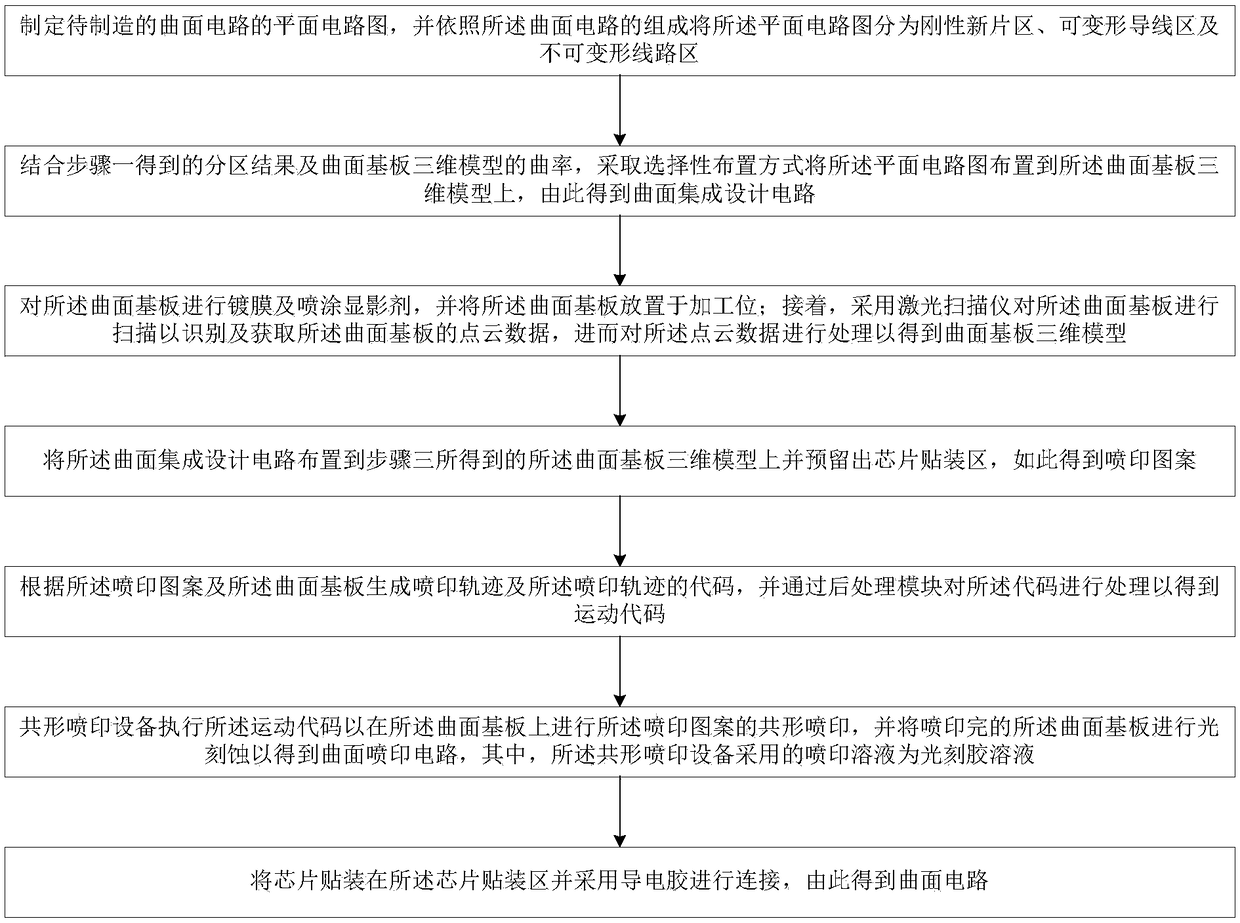
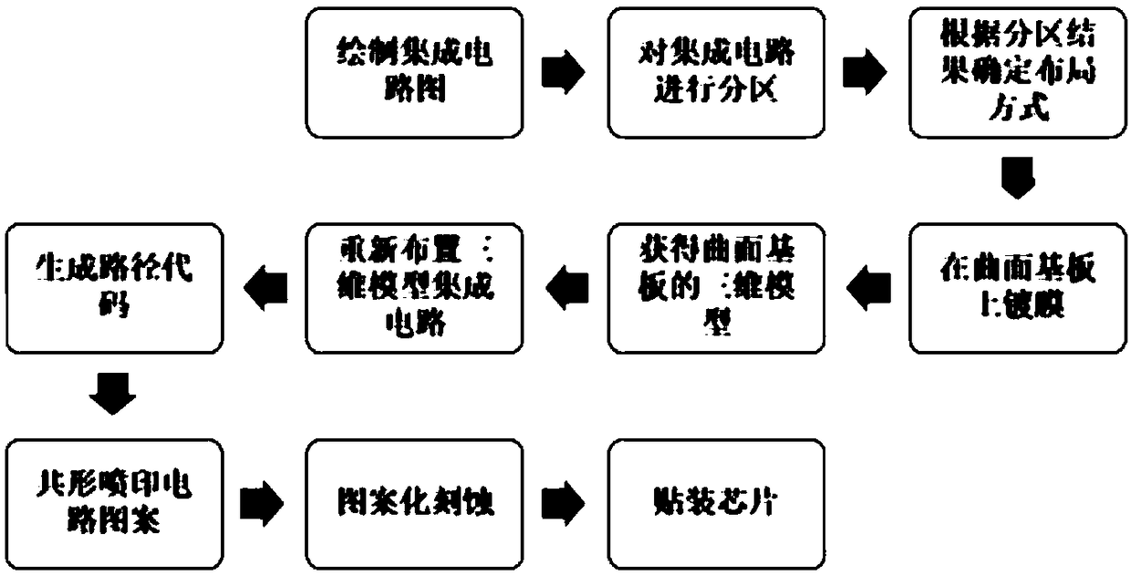
[0041] see figure 1 , the electrofluid jet printing and etching method for manufacturing curved surface integrated circuits provided by the first embodiment of the present invention, the method mainly includes the following steps:

[0042] Step 1, formulate the planar circuit diagram of the curved surface integrated circuit to be manufactured, and divide the planar circuit diagram into a rigid ...


PUM


Abstract

The invention belongs to the technical field related to the manufacture of curved surface integrated circuits, and discloses an electro-hydrodynamic jet etching method for manufacturing the curved surface integrated circuits. The method comprises the following steps: (1) preparing a plane circuit diagram of the curved surface integrated circuits and partitioning the plane circuit diagram; 2, arranging a plane circuit diagram on a three-dimensional model of a curved surface substrate to obtain a curved surface integrate design circuit; (3) scanning the coated curved surface substrate to identify and obtain the point cloud data of the curved surface substrate, and then obtaining a three-dimensional model of the curved surface substrate; 4) arranging a curved surface integrate design circuiton a three-dimensional model of a new curved surface substrate to obtain a jet printing pattern; (5) generating a code of the jet printing trajectory, and further obtaining a motion code; 6) allowingthat conformal jet prin device to execute a motion code to perform conformal jet printing, and etching the printed curved surface substrate to obtain a curved surface jet print circuit; and 6) allowing the conformal jet printing device to execute motion code to perform conformal jet printing and etching the printed curved surface substrate to obtain a curved surface jet printing circuit; (7) mounting the chip to obtain a curved surface integrated circuit. The invention improves the integration level, has good applicability and high manufacturing accuracy.

Description

technical field [0001] The invention belongs to the technical field related to the manufacture of curved integrated circuits, and more particularly relates to an electrofluid jet printing and etching method for manufacturing curved integrated circuits. Background technique [0002] Curved integrated circuits refer to the deposition of inorganic / organic materials on curved substrates to form electronic devices with corresponding functions, and then form integrated electronic systems. With the promotion of curved surface electronic products and the continuous development and improvement of microelectronics manufacturing technology, the preparation of electronic devices has gradually developed from traditional silicon-based or glass-based flat substrates to curved surface substrates, thus giving birth to many new application fields, such as curved surface Displays, conformal antennas, smart skins and electronic skins, etc. [0003] Curved surface integrated circuits have advan...

Claims


Application Information

Patent Timeline
Patent Type & Authority Applications(China)
IPC IPC(8): H01L21/48
CPCH01L21/4846
Inventor 黄永安朱慧吴昊尹浪
Owner HUAZHONG UNIV OF SCI & TECH
Why Eureka
Try Eureka