Sensitive amplifier circuit

A technology of sensitive amplifiers and circuits, which is applied to amplifiers, amplifiers with field effect devices, amplifiers with only semiconductor devices, etc., can solve the problems of the influence of charging speed and the longer acceleration time of the latch circuit, and achieve the goal of increasing the speed Effect

Active Publication Date: 2019-01-22
SHANGHAI HUAHONG GRACE SEMICON MFG CORP
View PDF8 Cites 1 Cited by
  • Summary
  • Abstract
  • Description
  • Claims
  • Application Information

AI Technical Summary

Problems solved by technology

[0007] exist figure 1 In the circuit shown, the voltage of node VE during charging is VDD-Vt, VDD is the power supply voltage, and Vt is the threshold voltage of the PMOS transistor PM1, which will affect the charging speed. In addition, when Iref and Icell are close, the latch The time for the circuit to accelerate will be longer

Method used


Image

  • Sensitive amplifier circuit
  • Sensitive amplifier circuit
  • Sensitive amplifier circuit

Examples


Embodiment Construction

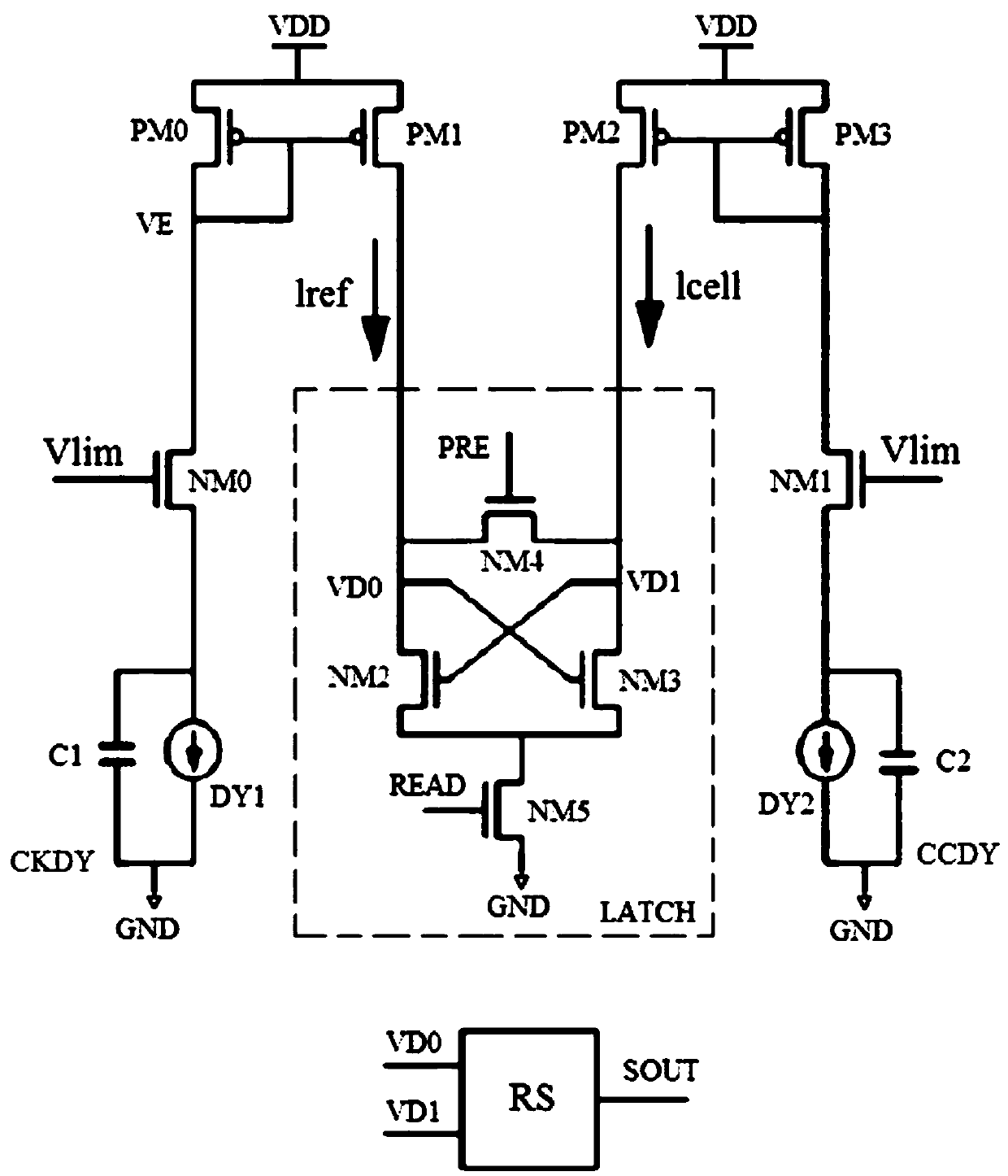
[0027] combine image 3 As shown, the improved sense amplifier circuit of the present invention, in the following embodiment, includes: nine PMOS transistors PM1-PM9, seven NMOS transistors NM1-NM7, two capacitors C1, C2, two inverters FX1 , FX2, an operational amplifier YF1, a voltage-controlled current source DY3 and a storage unit.

[0028] The sources of the PMOS transistors PM1 and PM4 and the drains of the PMOS transistors PM3 and PM2 are connected to the power supply voltage terminal VDD.

[0029] The source of the PMOS transistor PM3 is connected to the drain of the PMOS transistor PM1, and the connected node is denoted as LD. The source of the PMOS transistor PM2 is connected to the drain of the PMOS transistor PM4, and the connected node is denoted as RD. One end of the capacitor C1 is connected to the node LD, and the other end is connected to the gate of the PMOS transistor PM2, and the connected node is denoted as RG; one end of the capacitor C2 is connected to t...


PUM


Abstract

The invention discloses a sensitive amplifier circuit, which comprises nine PMOS transistors, seven NMOS transistors, two capacitors, two inverters, an operational amplifier, a voltage-controlled current source and a memory cell. The first capacitor and the second capacitor control compensation currents of the first PMOS transistor and the second PMOS transistor. A memory cell current and a firstvoltage control current source current influence a compensation current through a first capacitor and a second capacitor, thereby realize that function of dynamically changing the compensation current. The invention can greatly increase the speed of the comparison current and realize the high-speed sensitive amplifier circuit.

Description

technical field [0001] The invention relates to the field of semiconductor integrated circuits, in particular to a sense amplifier (SA) circuit. Background technique [0002] The traditional sense amplifier mainly achieves the effect of increasing the speed through the method of current comparison and acceleration of the latch. [0003] figure 1 It is an existing traditional sensitive amplifier circuit, which consists of four PMOS transistors PM0~PM3, six NMOS transistors NM0~NM5, two capacitors C1, C2, two voltage-controlled current sources DY1, DY2, an RS flip-flop RS composition. [0004] The current lref is the current flowing out from the drain of the PMOS transistor PM1 and entering the node VD0; the current lcell is the current flowing out of the drain of the PMOS transistor PM2 and entering the node VD1. [0005] LATCH is a latch circuit, and the reference storage unit CKDY is in figure 1 C is composed of a capacitor C1 and a voltage-controlled current source DY1...

Claims


Application Information

Patent Timeline
Patent Type & Authority Applications(China)
IPC IPC(8): H03F3/16
CPCH03F3/165
Inventor 王鑫
Owner SHANGHAI HUAHONG GRACE SEMICON MFG CORP
Why Eureka
Try Eureka